Method for manufacturing an electro-optical device

a manufacturing method and electro-optical technology, applied in the manufacture of electrode systems, cold cathode manufacturing, electric discharge tube/lamp manufacture, etc., can solve the problems of easy contamination of external atmosphere, difficult treatment, and extremely difficult patterning, and achieve high reliability, good operation performance, and increase the quality of electronic equipment

Inactive Publication Date: 2005-09-08
SEMICON ENERGY LAB CO LTD
View PDF99 Cites 96 Cited by
  • Summary
  • Abstract
  • Description
  • Claims
  • Application Information

AI Technical Summary

Benefits of technology

[0010] The present invention is made in view of the above problems, and an object of the present invention is to provide a method for manufacturing an electro-optical device having good operation performance and high reliability, and in particular, to provide a meth

Problems solved by technology

However, most of the materials used in general as EL layers are organic materials and the patterning is extremely difficult.
This is because EL materials themselves are very weak to moisture, and it is difficult to treat them as they easily dissolve even in a developing solution.
However, because ink jet method is performed

Method used


Image

  • Method for manufacturing an electro-optical device
  • Method for manufacturing an electro-optical device
  • Method for manufacturing an electro-optical device

Examples


embodiment 1

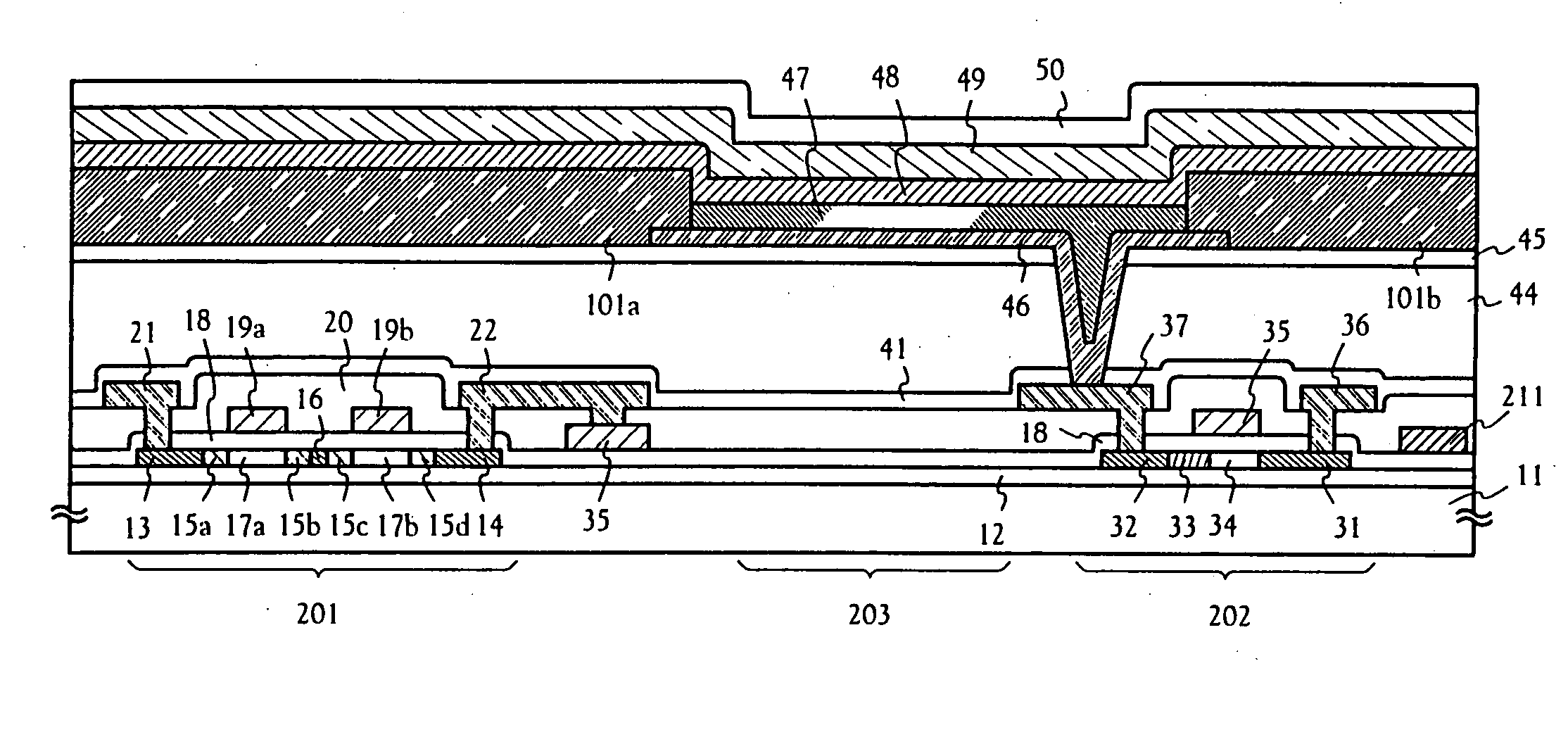
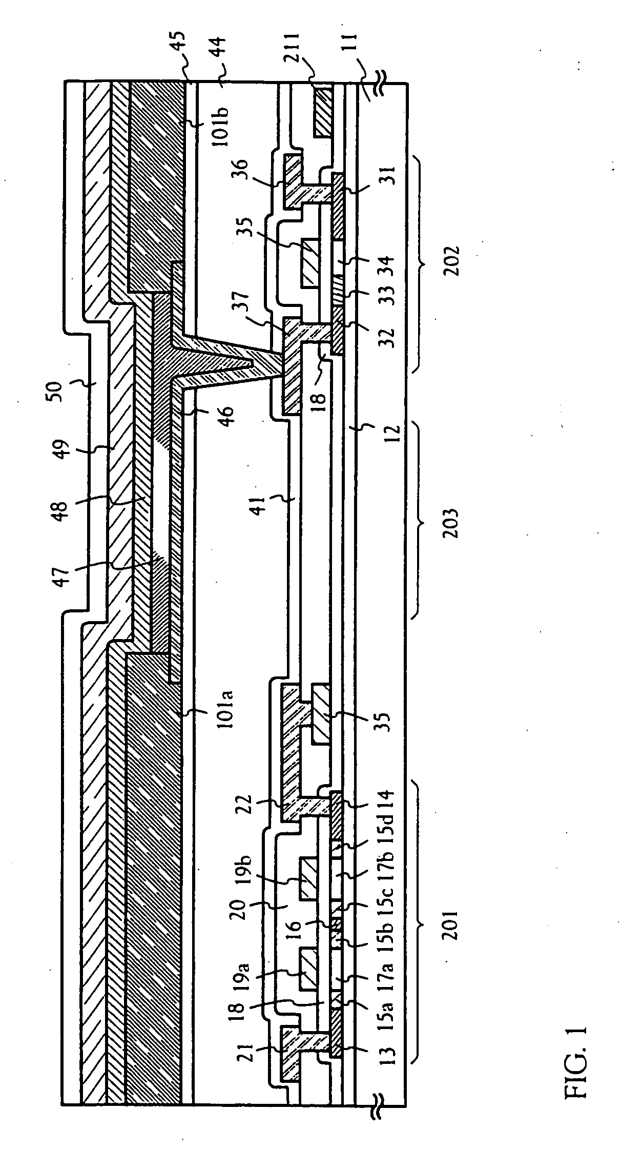
[0126] The embodiments of the present invention are explained using FIGS. 3A to 5C. A method of manufacturing a pixel portion, and TFTs of a driver circuit portion formed in the periphery of the pixel portion, is explained here. Note that in order to simplify the explanation, a CMOS circuit is shown as a basic circuit for the driver circuits.

[0127] First, as shown in FIG. 3A, a base film 301 is formed with a 300 nm thickness on a glass substrate 300. Silicon nitride oxide films are laminated as the base film 301 in embodiment 1. It is good to set the nitrogen concentration to between 10 and 25 wt % in the film contacting the glass substrate 300.

[0128] Further, it is effective to form an insulating film made from the same material as that of the first passivation film 41 shown in FIG. 1, as a portion of the base film 301. A large electric current flows in a current control TFT, heat is easily generated, and therefore it is effective to form an insulating film that has a heat radiat...

embodiment 2

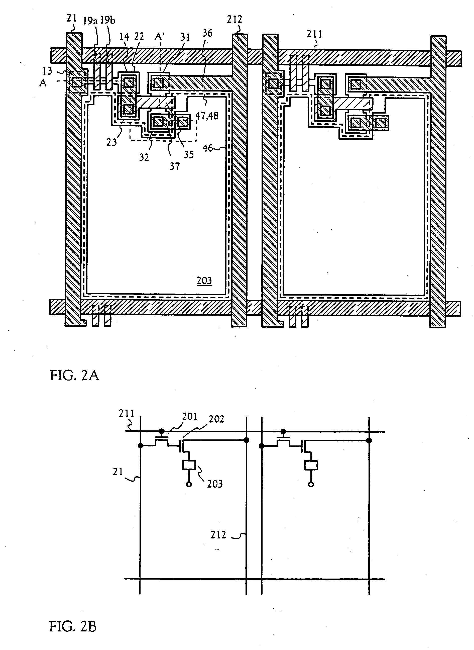
[0209] In this embodiment, an example in which a structure of a pixel is made different from the structure shown in FIG. 2B will be described with reference to FIG. 10.

[0210] In this embodiment, two pixels shown in FIG. 2B are arranged to become symmetrical with respect to a current supply line. That is, as shown in FIG. 10, a current supply line 213 is made common to two adjacent pixels, so that the number of necessary wiring lines can be reduced. Incidentally, a TFT structure or the like arranged in the pixel may remain the same.

[0211] If such structure is adopted, it becomes possible to manufacture a more minute pixel portion, and the quality of an image is improved.

[0212] Incidentally, the structure of this embodiment can be easily realized in accordance with the manufacturing steps of the embodiment 1, and with respect to the TFT structure or the like, the description of the embodiment 1 or FIG. 1 may be referred to.

embodiment 3

[0213] In this embodiment, a case where a pixel portion having a structure different from FIG. 1 will be described with reference to FIG. 11. Incidentally, steps up to a step of forming a second interlayer insulating film 44 may be carried out in accordance with the embodiment 1. Since a switching TFT 201 and a current controlling TFT 202 covered with the second interlayer insulating film 44 have the same structure as that in FIG. 1, the description here is omitted.

[0214] In the case of this embodiment, after a contact hole is formed through the second passivation film 45, the second interlayer insulating film 44, and the first passivation film 41, a pixel electrode 51 and banks 103a and 103b are formed, and then, a cathode 52 and an EL layer 53 are formed. In this embodiment, after the cathode 52 is formed by vacuum evaporation, the EL layer 53 is formed by an ink-jet method without exposure to the air while a dried inert atmosphere is kept. At this time, a red light emitting EL l...


PUM

PropertyMeasurementUnit
Lengthaaaaaaaaaa
Diameteraaaaaaaaaa

Abstract

An object of the present invention is to provide an EL display device having high operation performance and reliability.
A third passivation film 45 is disposed under the EL element 203 comprising a pixel electrode (anode) 46, an EL layer 47 and a cathode 48, and diffusion of alkali metals from the EL element 203 formed by ink jet method into TFTs is prevented. Further, the third passivation film 45 prevents penetration of moisture and oxygen from the TFTs, and suppress degradation of the EL element 203 by dispersing the heat generated by the EL element 203.

Description

BACKGROUND OF THE INVENTION [0001] 1. Field of the Invention [0002] The present invention relates to an electro-optical device, typically an EL (electroluminescence) display device formed by a semiconductor element (an element using a semiconductor thin film) made on a substrate, and to electronic equipment (an electronic device) having the electro-optical device as a display (also referred to as a display portion). In particular, the present invention relates to a manufacturing method thereof. [0003] 2. Description of the Related Art [0004] Techniques of forming a TFT on a substrate have been widely progressing in recent years, and developments of applications to an active matrix type display device are advancing. In particular, a TFT using a polysilicon film has a higher electric field effect mobility (also referred to as mobility) than a TFT using a conventional amorous silicon film, and high speed operation is therefore possible. As a result, it becomes possible to perform pixel...

Claims


Application Information

Patent Timeline
IPC IPC(8): C09K11/06H01L21/77H01L29/786H01L27/12H01L27/32H01L51/00H01L51/52H05B33/10H05B33/22
CPCH01L27/12H01L51/52H01L27/3211H01L27/3244H01L27/3258H01L51/0005H01L51/0038H01L51/0042H01L51/0059H01L51/0062H01L51/0077H01L51/0078H01L51/0081H01L51/0085H01L51/0087H01L51/5237H01L51/529H01L27/1214H10K59/35H10K59/12H10K59/124H10K71/135H10K85/146H10K85/114H10K85/649H10K85/631H10K85/311H10K85/30H10K85/346H10K85/324H10K85/342H10K50/841H10K50/84H10K50/844H10K50/87H01L29/786H10K50/80
Inventor YAMAZAKI, SHUNPEIKOYAMA, JUNYAMAMOTO, KUNITAKAKONUMA, TOSHIMITSU
Owner SEMICON ENERGY LAB CO LTD
Why Eureka
Try Eureka