Phosphorescent compound and organic light emitting diode device using the same
一种化合物、磷光的技术,应用在OLED器件领域,能够解决发光产率降低等问题
- Summary
- Abstract
- Description
- Claims
- Application Information
AI Technical Summary
Problems solved by technology
Method used
Image
Examples
Embodiment
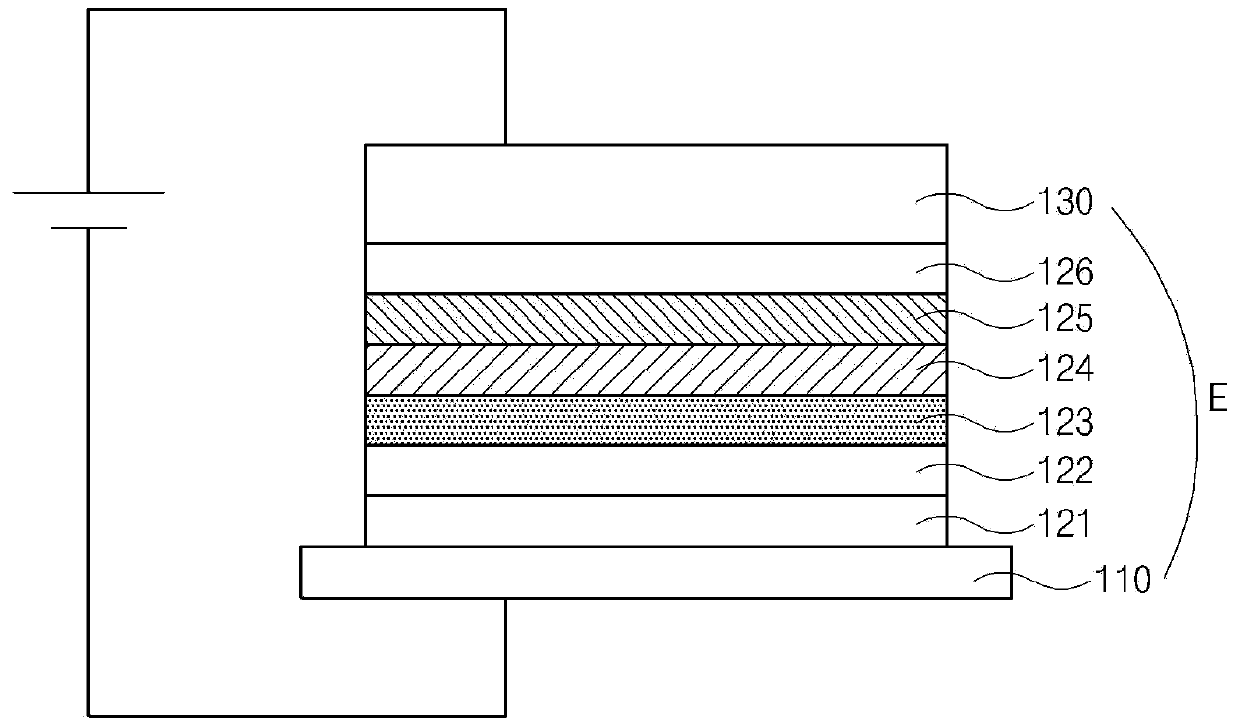
[0068] An ITO layer was deposited on the substrate and patterned to have an area of 3 mm x 3 mm, then washed to form the anode. Load the substrate into a vacuum chamber, and sequentially form a hole injection layer of hexaazatriphenanthrene-hexanitrile (HAT-CN) on the anode Hole-transporting layer of 4-4'-bis[N-(1-naphthyl)-N-phenylamino]biphenyl (NPB) Electron blocking layer of bis(4-(N,N'-xylylamino)phenyl)cyclohexane (TAPC) Emitting material layer of "A-1" phosphorescent compound and FCNIr blue dopant (15%) in formula 5 above Electron transport layer of TmPyPB Electron injection layer of LiF and aluminum cathode
PUM
 Abstract
Description
Claims
Application Information
 - R&D
- Intellectual Property
- Life Sciences
- Materials
- Tech Scout
- Unparalleled Data Quality
- Higher Quality Content
- 60% Fewer Hallucinations
Browse by: Latest US Patents, China's latest patents, Technical Efficacy Thesaurus, Application Domain, Technology Topic, Popular Technical Reports.
© 2025 PatSnap. All rights reserved.Legal|Privacy policy|Modern Slavery Act Transparency Statement|Sitemap|About US| Contact US: help@patsnap.com


