

Collection method of etching conditions
A collection method and conditional technology, which is applied in the direction of electrical components, electric solid-state devices, semiconductor devices, etc., can solve the problems of cost increase, wafer cost increase, wafer waste, etc., and achieve the goal of improving utilization, avoiding waste, and reducing costs Effect
- Summary
- Abstract
- Description
- Claims
- Application Information
AI Technical Summary
Problems solved by technology
Method used
Image

Examples
Embodiment 1
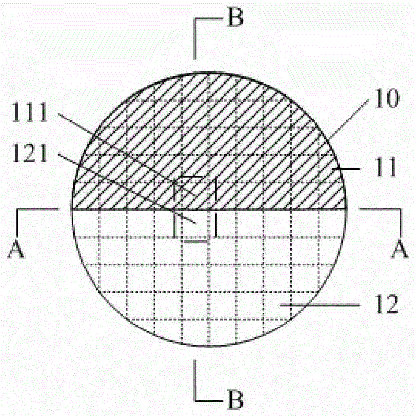
[0042] refer to figure 2 , is a top view of the wafer 10, and the wafer 10 includes several device regions.
[0043] In this embodiment, a silicon germanium layer may also be formed on the surface of the wafer 10 , and semiconductor devices (such as MOS devices, etc.) may also be formed in the wafer 10 .
[0044] continue to refer figure 2 , dividing the wafer 10 into two types of etching regions.
[0045] In this embodiment, the wafer 10 is divided into two types of etching regions: a first-type etching region 11 and a second-type etching region 12 along any diameter of the wafer 10 (for example: AA direction).
[0046] It should be noted that the present invention does not limit the method of dividing the wafer 10 into several types of etching regions and the number of device regions in each type of etching region, such as dividing the wafer 10 along a concentric circle with the circumference of the wafer 10 At least two types of etching regions that are divided into ri...
Embodiment 2
[0070] refer to Figure 8 , is a top view of the wafer 13, and the wafer 13 includes several device regions.
[0071] continue to refer Figure 8 , the wafer 13 is divided into four types of etching areas along its two mutually perpendicular diameter directions, which are respectively the first type etching area 14, the second type etching area 15, and the third type etching area. region 16 and the fourth type etched region 17 .
[0072] For the convenience of description, the device regions 141, 151, 161 and 171 are respectively selected from the above four types of etching regions 14, 15, 16 and 17, and the method for collecting etching conditions of the present invention is described.
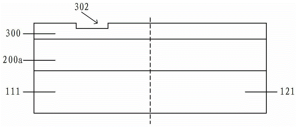
[0073] Figure 9A is a cross-sectional view of the device regions 141 and 151 along the CC direction, Figure 9B is a cross-sectional view of the device regions 161 and 171 along the DD direction, combined with reference Figure 9A and 9B ,exist Figure 8A dielectric layer 201 a and a...
PUM
 Abstract
Description
Claims
Application Information