Preparation method of fes2 thin film

A thin film, fe2o3 technology, applied in the field of FeS2 thin film and its preparation, can solve the problems of low photoelectric conversion efficiency and poor light absorption performance, and achieve the effect of increasing effective light absorption area, improving photoelectric conversion efficiency, and enhancing light absorption performance

Inactive Publication Date: 2016-05-11
ZHEJIANG UNIV
View PDF2 Cites 0 Cited by
  • Summary
  • Abstract
  • Description
  • Claims
  • Application Information

AI Technical Summary

Problems solved by technology

[0006] In order to overcome the shortcomings of poor light absorption performance and low photoelectric conversion efficiency of the existing iron disulfide film, the present invention provides a method to improve the light absorption performance and photoelectric conversion efficiency of the iron disulfide film by increasing the effective light absorption area. Iron disulfide nanotube array thin film with conversion efficiency and preparation method thereof

Method used


Image

  • Preparation method of fes2 thin film
  • Preparation method of fes2 thin film
  • Preparation method of fes2 thin film

Examples


Embodiment 1

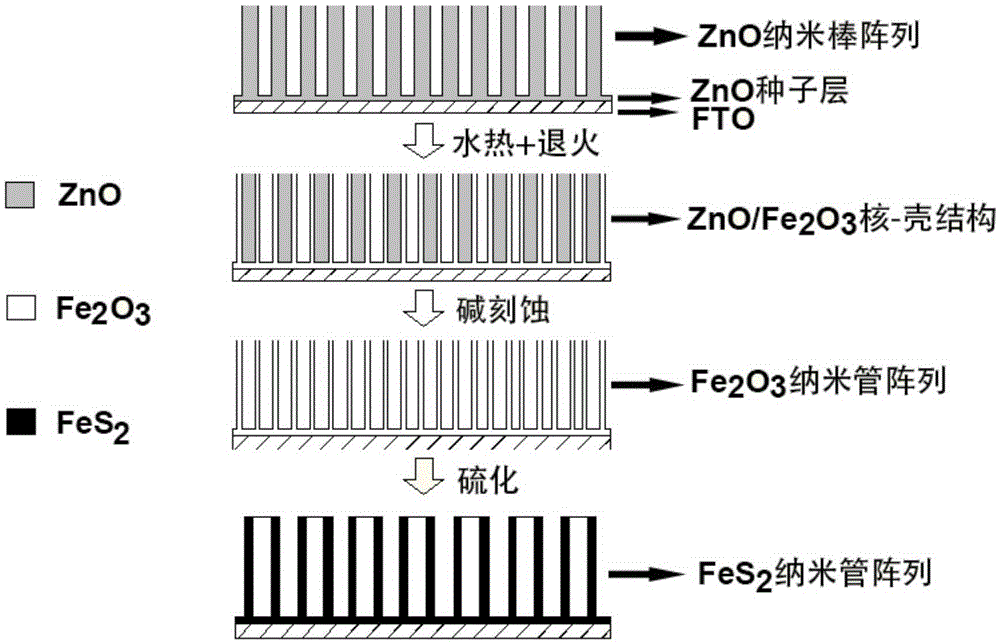
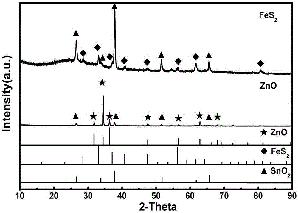
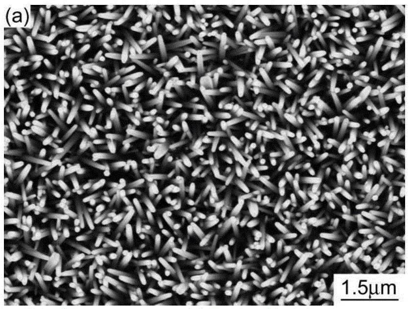
[0037] combined with Figure 1-4 , to further illustrate the present invention:

[0038] a FeS 2 The preparation method of thin film, comprises the following steps:

[0039] 1) Substrate pretreatment: In this example, the size is The conductive glass is used as the substrate, but the size of the substrate is not limited to the example of this embodiment. The substrate was ultrasonically cleaned in acetone solution for 20 minutes, then ultrasonically cleaned in absolute ethanol for 20 minutes, and finally ultrasonically cleaned in deionized water for 20 minutes; the cleaned substrate was dried in a constant temperature drying oven at 100°C, and the dried Base spare;

[0040] 2) Pour 50ml of ethylene glycol methyl ether solvent into a beaker, add 0.05mol of zinc acetate dihydrate and 3ml of ethanolamine, stir magnetically at a constant temperature of 60°C for 30min until completely dissolved, and form a uniform and transparent seed layer solution; magnetically stir The pur...

Embodiment 2

[0049] Such as Figure 4 , 5 As shown, a FeS 2 Thin film, including FTO conductive glass substrate 1, covered with FeS on the substrate 1 2 nanotube array, each FeS 2 Nanotube 2 made of FeS 2 The particles 21 are piled up.

[0050] by FeS 2 One-dimensional ordered FeS composed of nanoparticles 2 The nanotube array structure makes the FeS 2 The film has a three-dimensional structure, which enables the use of FeS 2 The inner and outer surfaces of the nanotubes undergo light absorption, greatly increasing the FeS 2 The light absorption area of ​​the film; compared with conventional FeS 2 Nanoparticle films compared to one-dimensionally ordered FeS 2 Nanotube array structure has enhanced FeS 2 effective light absorption area of ​​the film, increasing the FeS 2 The light-absorbing properties of thin films are improved by FeS 2 Advantages of thin-film photoelectric conversion efficiency.


PUM

PropertyMeasurementUnit
thicknessaaaaaaaaaa
electrical resistanceaaaaaaaaaa
thicknessaaaaaaaaaa

Abstract

The invention provides a preparation method of a FeS2 thin film. The method includes the first step of using FTO conductive glass as a substrate, the second step of forming uniform and transparent seed layer solution, the third step of forming a uniform ZnO nanometer crystal seed layer on the surface of the substrate, the fourth step of preparing precursor solution, the fifth step of forming a uniform and dense ZnO nanorod array on the surface of the substrate, the sixth step of placing the substrate provided with the ZnO nanorod array into the precursor solution in a reaction still for hydrothermal reaction, and forming a ZnO / Fe2O3 core-shell structure nanorod array on the surface of the substrate, the seventh step of obtaining a Fe2O3 nanotube array on the surface of the substrate, and the eighth step of carrying out in-situ sulphur treatment on the Fe2O3 nanotube array and converting the Fe2O3 nanotube array to a FeS2 nanotube array. The FeS2 thin film comprises the FTO conductive glass substrate, the substrate is covered with the FeS2 nanotube array, and each FeS2 nanotube is formed by accumulating FeS2 particles. The method has the advantages that the effective light absorption area of the FeS2 thin film can be increased, so that the light absorption performance and the photoelectric conversion efficiency of the FeS2 thin film are improved.

Description

technical field [0001] The invention relates to the field of photoelectric materials and new energy technologies, in particular to a FeS 2 Thin films and methods for their preparation. technical background [0002] With the outbreak of the economic crisis in 2008 and the intensification of Sino-US photovoltaic trade frictions, the development of the global photovoltaic industry has slowed down and faced a serious crisis, causing most photovoltaic companies to go bankrupt or bear heavy economic burdens. The root cause is cost. Therefore, cost reduction is an important factor that must be considered for any solar material. At this stage, the conversion efficiency of crystalline silicon solar cells is undoubtedly the highest, and it still occupies a dominant position in large-scale applications and industrial production. However, the high cost of raw silicon and the scarcity of resources have limited the future development of silicon solar cells, and at the same time, compou...

Claims


Application Information

Patent Timeline
Patent Type & Authority Patents(China)
IPC IPC(8): H01L31/20H01L31/0296
CPCH01L31/032H01L31/18Y02P70/50
Inventor 汪牡丹刘嘉斌黄六一孟亮
Owner ZHEJIANG UNIV
Why Eureka
Try Eureka