Magnetic field controlled silicon-based non-volatile resistance variable device and preparation method thereof

A non-volatile, resistive device technology, applied in electrical components and other directions, can solve the problems of no magnetoresistance effect and inability to magnetic sensing, and achieve the effect of significant magnetoresistance effect, simple preparation process and moderate price

Inactive Publication Date: 2014-06-25
TSINGHUA UNIV
View PDF3 Cites 0 Cited by
  • Summary
  • Abstract
  • Description
  • Claims
  • Application Information

AI Technical Summary

Problems solved by technology

But it does not have the magnetoresistive effect and cannot be used as a magnetic sensor

Method used


Image

  • Magnetic field controlled silicon-based non-volatile resistance variable device and preparation method thereof
  • Magnetic field controlled silicon-based non-volatile resistance variable device and preparation method thereof
  • Magnetic field controlled silicon-based non-volatile resistance variable device and preparation method thereof

Examples


Embodiment 1

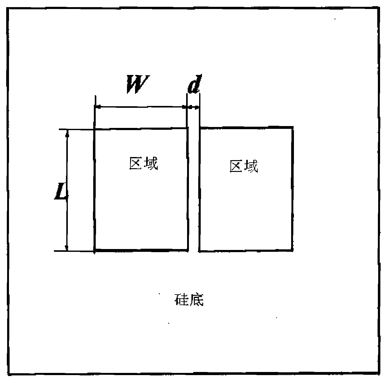
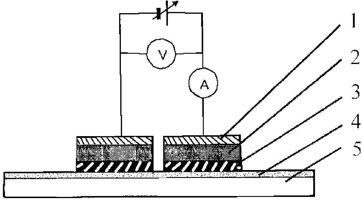
[0035] Rinse the n-type silicon (111) and the substrate with a resistivity of 3200Ω·cm with alcohol or acetone, and cut it into a length of 11.0×12.0mm 2 rectangle. At room temperature (300K) and cavity pressure of 1.8×10 by using a mask and laser pulse deposition method -4 Deposit 20nm thick high-purity MgO (purity>99.995%), 60nm thick high-purity Mg (purity>99.99%) and 20nm thick high-purity Ag (purity>99.99%) in the center of the rectangular silicon substrate in sequence under Pa. The dimensions of the two regions are the same, L=2mm in the length direction, W=1.5mm in the width direction, and d=0.1mm apart in the width direction. So far, a silicon-based nonvolatile resistive switching device with controllable magnetic field has been prepared.

Embodiment 2

[0037] Rinse the n-type silicon (100) substrate with a resistivity of 4000Ω·cm with alcohol or acetone, and cut it into a length of 11.0×12.0mm 2 rectangle. At room temperature (300K) and cavity pressure of 1.8×10 by using a mask and laser pulse deposition method -4 Deposit 40nm thick high-purity MgO (purity>99.995%), 80nm thick high-purity Mg (purity>99.99%) and 40nm thick high-purity Ag (purity>99.99%) in the center of the rectangular silicon substrate in sequence under Pa. The dimensions of the two regions are the same, L=1.8mm in the length direction, W=1.2mm in the width direction, and d=0.5mm apart in the width direction. So far, a silicon-based non-volatile resistive device with controllable magnetic field has been prepared.


PUM

PropertyMeasurementUnit
Thicknessaaaaaaaaaa
Resistivityaaaaaaaaaa
Mobilityaaaaaaaaaa

Abstract

The invention discloses the structure of a magnetic field controlled silicon-based non-volatile resistance variable device and a preparation method thereof, belonging to the field of magnetic field controlled and memory manufacturing technology. According to the magnetic field controlled silicon-based non-volatile resistance variable device, two MgO areas are arranged at the surface of a rectangular monocrystaline silicon substrate, and metal electrodes with the same area are orderly deposited on MgO. The preparation method comprises the steps of cutting the rectangular monocrystaline silicon substrate into a rectangular shape, washing the substrate with acetone, alcohol and deionized water in order, depositing two MgO areas at the surface of a rectangular monocrystaline silicon substrate, and depositing the metal electrodes on the MgO to obtain the magnetic field controlled silicon-based non-volatile resistance variable device. The obtained magnetic field controlled silicon-based non-volatile resistance variable device has a significant non-volatile resistance variable characteristic and can be controlled by a magnetic field to exhibit or not exhibit the resistance variable characteristic, and the device has a magnetic reluctance characteristic at the same time. The magnetic field controlled silicon-based non-volatile resistance variable device has the advantages of simple structure, moderate price of raw materials, simple preparation process, and environmental friendliness.

Description

technical field [0001] The invention belongs to the technical fields of magnetic field control and memory preparation, and in particular relates to a magnetic field controllable silicon-based non-volatile resistive switch device and a preparation method. Background technique [0002] Non-volatile RRAM has become the best candidate device for next-generation data storage because of its fast read and write speed, large capacity, low energy consumption and multi-bit storage (Mater.Today.11(2008) 28) . At present, the main non-volatile RRAMs are all metal / oxide / metal structures, and the main working oxides are simple binary oxides such as NiO, ZnO and TiO 2 etc., and multiple oxides such as PrCaMnO 3 (PCMO), etc. In addition, the most important and most commonly used semiconductor silicon in the semiconductor industry is also used to prepare non-volatile resistive memory. However, amorphous silicon is mostly used, while very few nonvolatile RRAMs are prepared using crystalli...

Claims


Application Information

Patent Timeline
IPC IPC(8): H01L45/00
Inventor 章晓中王集敏朴红光罗昭初熊成悦
Owner TSINGHUA UNIV
Why Eureka
Try Eureka