Light modulator with four-layer graphene structure

A layer graphene, light modulator technology, applied in the field of optoelectronics, can solve problems such as small switching time, achieve the effects of small capacitance and resistance, reduce volume, and shorten the length of the active region

Inactive Publication Date: 2014-07-02
UNIV OF ELECTRONICS SCI & TECH OF CHINA
View PDF6 Cites 15 Cited by
  • Summary
  • Abstract
  • Description
  • Claims
  • Application Information

AI Technical Summary

Problems solved by technology

[0007] In order to meet the requirements of future optical fiber communication technology, the optical modulator should have higher modulation speed, shorter ...

Method used


Image

  • Light modulator with four-layer graphene structure
  • Light modulator with four-layer graphene structure
  • Light modulator with four-layer graphene structure

Examples


Embodiment

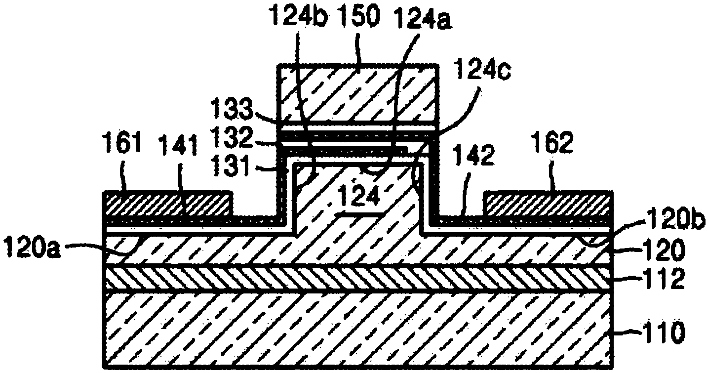
[0042] figure 1 It is a cross-sectional view of the optical modulator in the invention patent "Optical Modulator Including Graphene" (application number CN201210397252.3) filed by South Korea's Samsung Electronics Co., Ltd. in China in 2012. The length of its active area is 35μm, and the 3dB modulation bandwidth f3dB=55GHz.

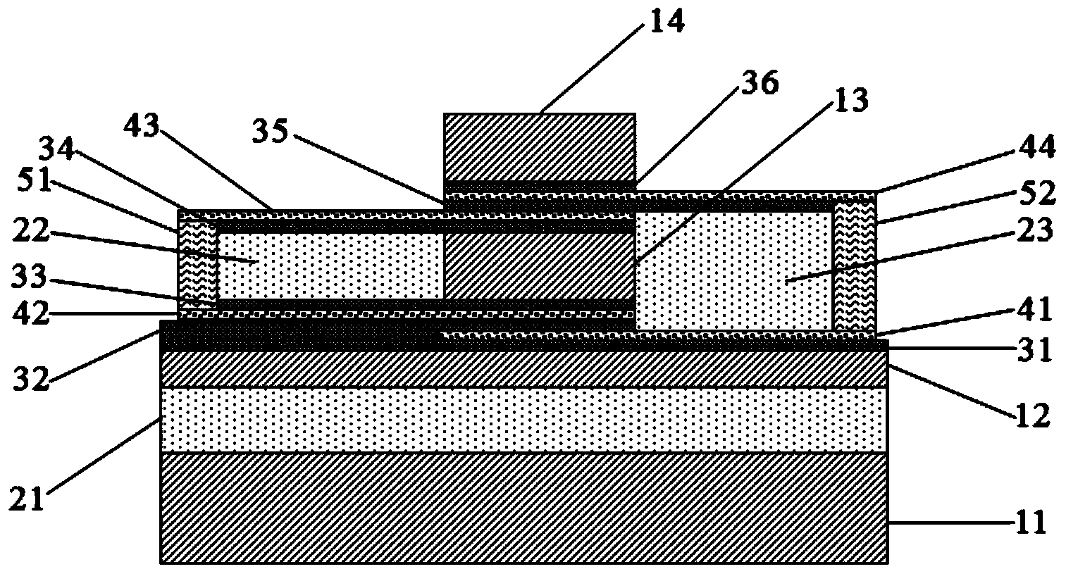
[0043] figure 2 is a structural schematic diagram of the light modulator with four-layer graphene structure of the present invention. In this embodiment, light waves with a wavelength of 1.55 μm are used. The semiconductor substrate layer 11, the semiconductor optical waveguide layer 12, the first ridge 13, and the second ridge 14 are made of silicon (Si) material (refractive index 3.47), and the width of the first ridge 13 and the second ridge 14 is 0.4 μm, the thickness is 0.13 μm; the insulating layer 21, the first filling medium 22 and the second filling medium 23 are silicon dioxide (SiO 2 ) material (refractive index 1.444), the thickness of th...


PUM


Abstract

The invention discloses a light modulator with a four-layer graphene structure and belongs to the field of photoelectronic techniques. The light modulator comprises an SOI light guide, a first ridge part and a second ridge part overlapping the first ridge part are arranged above a semiconductor light guide layer of the SOI light guide, two graphene layers are arranged between the semiconductor light guide layer and the first ridge part, another two graphene layers are arranged between the first ridge part and the second first ridge part, and all the functional layers are isolated from one another through isolation media; one graphene layer between the semiconductor light guide layer and the first ridge part is connected with one graphene layer between the first ridge part and the second first ridge part through one metal electrode, and the other graphene layer between the semiconductor light guide layer and the first ridge part is connected with the other graphene layer between the first ridge part and the second first ridge part through another metal electrode. The light modulator has the advantages of being smaller in size, high in modulation rate and convenient to integrate, wherein the extinction ratio of a 5 micrometer active area is as high as 30 dB, and the modulation rate of a 3 dB modulation bandwidth is as high as 114.8 GHz.

Description

technical field [0001] The invention belongs to the technical field of optoelectronics, and relates to a light modulator, especially a light modulator with a graphene structure. Background technique [0002] The basic structure of the optical modulator includes an optical crystal (or optical waveguide), which is located in the middle of an electric field perpendicular to the direction of light transmission (the electric field can pass through two parallel sides corresponding to the optical crystal or optical waveguide). Add electrodes, and then add a bias voltage between the two electrodes to achieve). Due to the existence of the bias electric field, when the light passes through the optical crystal or the optical waveguide, its refractive index or absorption rate changes, thereby causing a change in the phase or amplitude of the output light, which is the basic working principle of the optical modulator. [0003] The optical modulator plays a vital role in the modulation o...

Claims


Application Information

Patent Timeline
IPC IPC(8): G02F1/035
Inventor 刘永叶胜威唐林峰王子帅唐雄贵陆荣国陈德军廖进昆
Owner UNIV OF ELECTRONICS SCI & TECH OF CHINA
Why Eureka
Try Eureka