pop packaging structure and manufacturing process

A technology of packaging structure and manufacturing process, applied in semiconductor/solid-state device manufacturing, electrical components, electric solid-state devices, etc., can solve problems such as difficult warpage, slippage, and difficult control of dislocation, so as to achieve easy filling and improve warpage The effect of music

Active Publication Date: 2016-06-01
NAT CENT FOR ADVANCED PACKAGING CO LTD
View PDF8 Cites 0 Cited by
  • Summary
  • Abstract
  • Description
  • Claims
  • Application Information

AI Technical Summary

Problems solved by technology

At present, it is very difficult to control the warpage of the PoP solution of the fan-out package using the molding process. The existing solutions are all to reduce the warpage from the aspects of material properties and the final shape of the molding; In addition, the slippage and shift caused by the expansion and contraction of the plastic packaging compound (EMC) are also difficult to control

Method used


Image

  • pop packaging structure and manufacturing process
  • pop packaging structure and manufacturing process
  • pop packaging structure and manufacturing process

Examples


Embodiment Construction

[0039] The present invention will be further described below in conjunction with specific drawings.

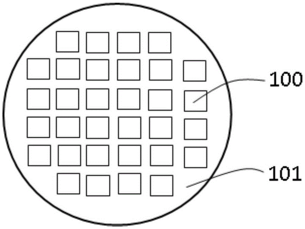
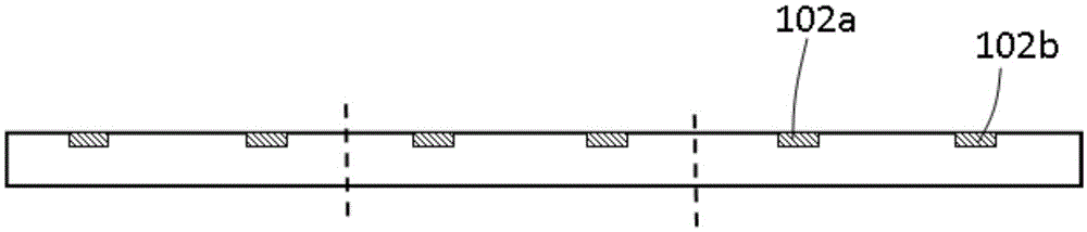
[0040] Such as Figure 13a , Figure 13b As shown: the PoP packaging structure includes upper and lower fan-out packaging units; the fan-out packaging unit includes a chip 100 with a first metal electrode 102a and a second metal electrode 102b and a metal layer 203, the chip 100 and The metal layer 203 is molded into a whole by the molding material 501; the front side 100a of the chip 100 is on the same plane as the front side 501a of the molding material 501, and the back side 100b of the chip 100 is on the same plane as the back side 501b of the molding material 501; Vertical through holes are made on the molding material 501 in the area where the layer 203 is located, and metal pillars 701 are formed by filling the vertical through holes. The first surface 701a of the metal pillars 701 is located on the same plane as the front surface 501a of the molding material 501, and ...


PUM


Abstract

The invention relates to a PoP packaging structure and manufacturing process, which is characterized in that, when the fan-out packaging unit is produced, the process flow of the chip facing up is adopted, and the metal layer is made on the carrier, and then slots are made according to the arrangement position of the chip And make electrodes interconnected with other packaging units according to the design requirements, thereby changing the internal structure of fan-out wafer level packaging, enhancing its rigidity and thermal expansion coefficient, making the warping of the entire wafer and the shrinkage caused by the expansion and contraction of the plastic packaging compound Slip and dislocation are under control. After plastic packaging, holes are opened on the back, filled with metal, and interconnected with the electrodes formed by the previous metal layer, and the metal layer is exposed on the back of the plastic packaging material after the carrier and adhesive layer are removed, and metal pads can be made. Such a package unit can be connected to other package units through a metal pad on the back of the package unit to form a multi-layer PoP package structure.

Description

technical field [0001] The invention relates to a PoP packaging structure and a manufacturing process, belonging to the technical field of semiconductor packaging. Background technique [0002] As the main way of packaging high-density integration at present, PoP (package on package, package on package) has received more and more attention. Chip stacking is the main way to increase the density of electronic packaging, and PoP design has been widely developed and applied in the industry. At present, it is very difficult to control the warpage of the PoP solution of the fan-out package using the molding process. The existing solutions are all to reduce the warpage from the aspects of material properties and the final shape of the molding; In addition, the slippage and shift caused by the expansion and contraction of the plastic encapsulant (EMC) are also difficult to control. Contents of the invention [0003] The purpose of the present invention is to overcome the deficie...

Claims


Application Information

Patent Timeline
Patent Type & Authority Patents(China)
IPC IPC(8): H01L23/538H01L23/31H01L21/768H01L21/56
CPCH01L24/19H01L2224/12105H01L2224/19H01L2224/73267H01L2224/94H01L2225/1035H01L2225/1058H01L2924/181H01L2924/18162H01L2924/00H01L2224/03H01L2924/00012
Inventor 王宏杰陈南南
Owner NAT CENT FOR ADVANCED PACKAGING CO LTD
Why Eureka
Try Eureka