

Three-dimensional fan-out type PoP packaging structure and manufacturing process
A packaging structure, fan-out technology, applied in semiconductor/solid-state device manufacturing, semiconductor/solid-state device components, semiconductor devices, etc., can solve problems such as difficult warping, slippage, and dislocation that are difficult to control, and achieve improvement warping effect
- Summary
- Abstract
- Description
- Claims
- Application Information
AI Technical Summary
Problems solved by technology
Method used
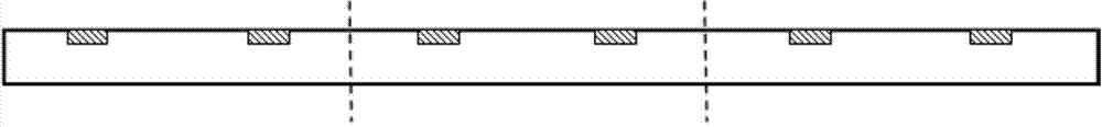
Image


Examples
Embodiment Construction
[0054] The present invention will be further described below in conjunction with specific drawings.
[0055] As shown in Figure 223a, Figure 22b As shown: the three-dimensional fan-out PoP packaging structure includes upper and lower layers of fan-out packaging units; Figure 21a , Figure 21b As shown, the fan-out packaging unit includes a first fan-out wafer level package 10, a second fan-out wafer level package 20 stacked on the front of the first fan-out wafer level package 10 and The backside rewiring layer 50 disposed on the backside of the first fan-out wafer level package 10 (the front side of the first fanout wafer level package 10 can be stacked in turn with one layer, two layers, three layers or four layers etc. layer second fan-out wafer level package body 20, Figure 21a , Figure 21b Only one stack is shown);
[0056] Such as Figure 21a , Figure 21b As shown, the first fan-out wafer level package 10 includes a first chip 101 with metal electrodes 1011, ...
PUM
 Abstract
Description
Claims
Application Information