Liquid crystal display module and liquid crystal display device

A technology of liquid crystal display module and display area, which is applied in the direction of instruments, printed circuits, printed circuits connected with non-printed electrical components, etc. , occupying the display area of ​​the display panel screen, etc., to improve the poor reliability of the packaging, reduce the risk of pressing offset, and improve the product yield.

Inactive Publication Date: 2019-04-09
WUHAN TIANMA MICRO ELECTRONICS CO LTD
View PDF5 Cites 15 Cited by
  • Summary
  • Abstract
  • Description
  • Claims
  • Application Information

AI Technical Summary

Problems solved by technology

[0002] In the field of liquid crystal display technology, the bonding of integrated circuit chips on the glass of the display panel (COG, Chip OnGlass) is a technology commonly used in current liquid crystal display modules, such as figure 1 The shown liquid crystal display module includes a display panel, the display panel includes a display area AA' and a non-display area BB', the integrated circuit chip I' is bound to the non-display area BB' of the display panel, and the liquid crystal display module also includes a flexible The circuit board F2' and the flexible circuit board F2' are bound to the non-display area BB' of the display panel through the binding terminal B1', but this method of directly binding the integrated circuit chip (IC) on the glass of the display panel will occupy the display panel. The screen display area is not conducive to the realization of the narrow frame full screen design of the liquid crystal display panel
In order to overcome this, the technology of binding integrated circuit chips on flexible circuit boards (COF, Chip On Film) is proposed, that is, the integrated circuit chips (IC) are first bound on the transfer flexible circuit boards, and then transferred to the flexible circuit boards. electrically connected to the main flex circuit board, as figure 2 shown in the LCD module, with figure 1 The difference is that the integrated circuit chip I' is bound to the transfer flexible circuit board F1', and one end of the transfer flexible circuit board F1' is bound to the non-display area BB' of the display panel through the binding terminal B1'. The other end of the circuit board F1' is bound to the flexible circuit board F2' through the binding terminal B2'. This double binding will cause a certain risk of pressing deviation, and the COF is easy to warp, which will lead to the reliability of the integrated circuit chip package. Poor and long ICs are directly tied to the soft single-layer transfer flexible circuit board. When the module is affected by external force or the module is manually taken, it is very easy to cause the IC to break, resulting in the scrapping of the entire module product and waste. resources and costs

Method used


Image

  • Liquid crystal display module and liquid crystal display device
  • Liquid crystal display module and liquid crystal display device
  • Liquid crystal display module and liquid crystal display device

Examples


Embodiment Construction

[0027] The following will clearly and completely describe the technical solutions in the embodiments of the present invention with reference to the accompanying drawings in the embodiments of the present invention. Obviously, the described embodiments are only some, not all, embodiments of the present invention. Based on the embodiments of the present invention, all other embodiments obtained by persons of ordinary skill in the art without making creative efforts belong to the protection scope of the present invention.

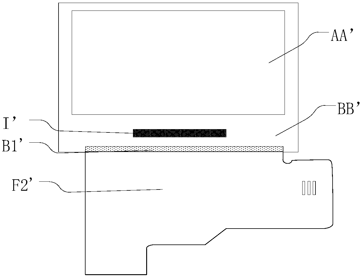
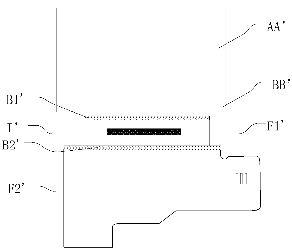
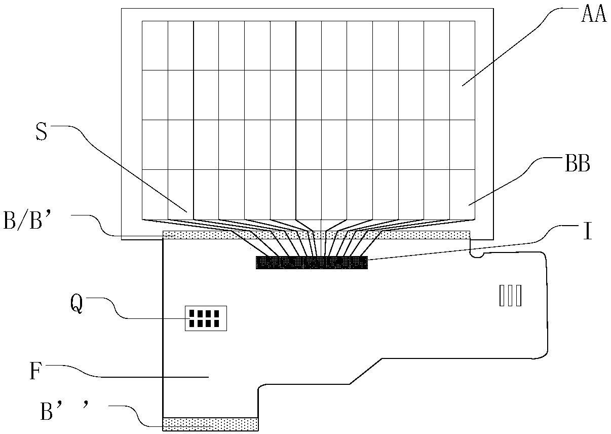
[0028] First, an embodiment of the present invention provides a liquid crystal display module, such as image 3 as shown, image 3 It is a schematic structural diagram of a liquid crystal display module provided by an embodiment of the present invention. The liquid crystal display module includes a display panel. The display panel includes a display area AA and a non-display area BB. The non-display area BB includes a first binding terminal B; The circuit boa...


PUM


Abstract

The present invention provides a liquid crystal display module and a liquid crystal display device. The liquid crystal display module comprises: a display panel; a flexible circuit board and an integrated circuit chip, wherein the flexible circuit board comprises a first end and a second end; the first end comprises a second binding terminal; the second binding terminal of the first end is connected to a first binding terminal of a non-display area; the flexible circuit board comprises at least two conductive layers; the flexible circuit board further comprises at least two rows of bonding pads between the first end and the second end; each row of the bonding pads comprises a plurality of sub-bonding pads; the conductive layers are exposed by the sub-bonding pads; the flexible circuit board further comprises a component group; and the integrated circuit chip is electrically connected to the sub-bonding pads through conductive adhesive. The module provided by the invention has the technical effects that the production efficiency can be improved; the cost is reduced; the risk of pressing deviation is reduced; the product yield is increased; the problem that the integrated circuit chip is easy to break is improved; and the package reliability of the integrated circuit chip is increased.

Description

technical field [0001] The invention relates to the display field, in particular to a liquid crystal display module and a liquid crystal display device. Background technique [0002] In the field of liquid crystal display technology, the bonding of integrated circuit chips on the glass of the display panel (COG, Chip OnGlass) is a technology commonly used in current liquid crystal display modules, such as figure 1 The shown liquid crystal display module includes a display panel, the display panel includes a display area AA' and a non-display area BB', the integrated circuit chip I' is bound to the non-display area BB' of the display panel, and the liquid crystal display module also includes a flexible The circuit board F2' and the flexible circuit board F2' are bound to the non-display area BB' of the display panel through the binding terminal B1', but this method of directly binding the integrated circuit chip (IC) on the glass of the display panel will occupy the display p...

Claims


Application Information

Patent Timeline
IPC IPC(8): G02F1/1345H05K1/18
CPCG02F1/13452G02F1/13458H05K1/189
Inventor 黄祥谭绿水光明星
Owner WUHAN TIANMA MICRO ELECTRONICS CO LTD
Why Eureka
Try Eureka