Pixel array substrate and tablet sensor comprising same

A pixel array substrate and pixel array technology, applied in the field of sensors, can solve problems such as poor electrostatic protection

Active Publication Date: 2014-07-16
SHANGHAI TIANMA MICRO ELECTRONICS CO LTD +1
View PDF6 Cites 14 Cited by
  • Summary
  • Abstract
  • Description
  • Claims
  • Application Information

AI Technical Summary

Problems solved by technology

[0005] In view of this, an embodiment of the present invention provides a pixel array substrate and a flat panel sensor including the same, to solve the technical problem in the prior art that the electrostatic protection structure of the flat panel sensor has poor electrostatic protection effect on the pixel units in the pixel array area

Method used


Image

  • Pixel array substrate and tablet sensor comprising same
  • Pixel array substrate and tablet sensor comprising same
  • Pixel array substrate and tablet sensor comprising same

Examples


Embodiment Construction

[0020] The present invention will be further described in detail below in conjunction with the accompanying drawings and embodiments. It should be understood that the specific embodiments described here are only used to explain the present invention, but not to limit the present invention. In addition, it should be noted that, for the convenience of description, only parts related to the present invention are shown in the drawings but not all content.

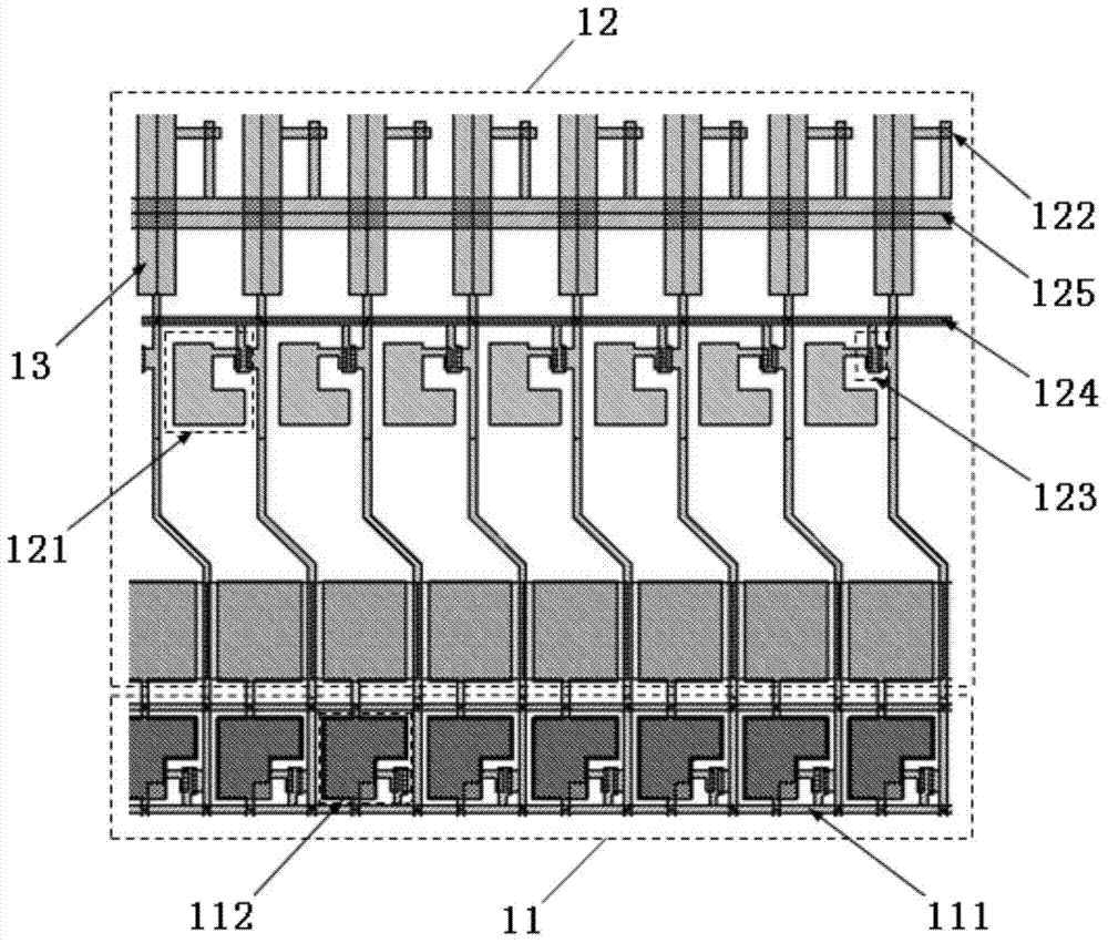
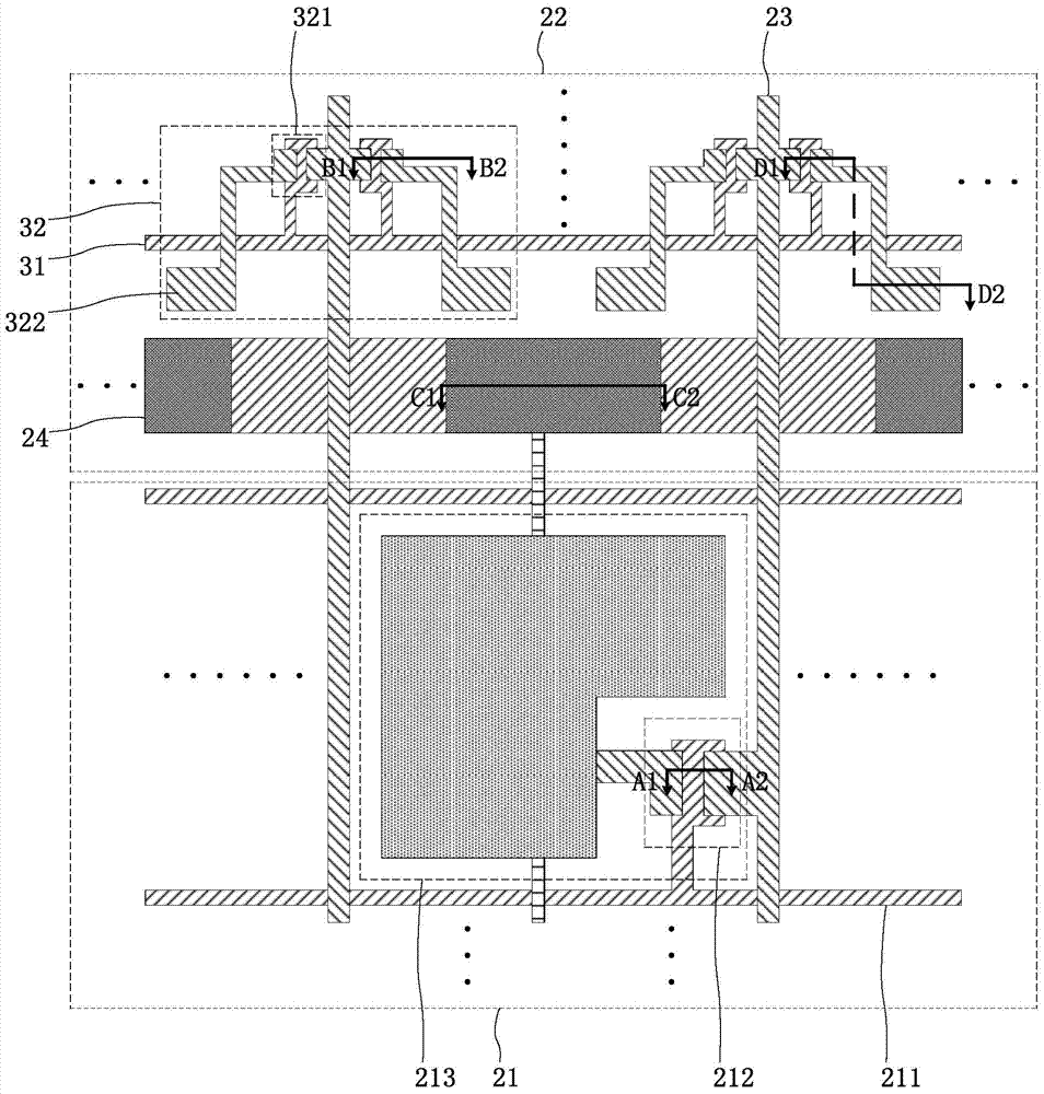
[0021] An embodiment of the present invention provides a pixel array substrate. figure 2 It is a schematic structural diagram of a pixel array substrate according to an embodiment of the present invention. see figure 2 The pixel array substrate includes: a pixel array area 21 and a peripheral area 22 surrounding the pixel array area 21; a plurality of data lines 23; a first scanning line 31 cross-insulated from the data lines 23 and located in the peripheral area 22 , and the peripheral area 22 also includes at least one e...


PUM


Abstract

The invention discloses a pixel array substrate and a tablet sensor comprising the pixel array substrate. The pixel array substrate comprises a pixel array area, a peripheral area, a plurality of data lines and a first scanning line, wherein the peripheral area surrounds the pixel array area, the first scanning line and the data lines intersect and are insulated, and the first scanning line is located in the peripheral area; the peripheral area further comprises at least one electrostatic protection unit, and all electrostatic protection units are located at the intersections between the data lines and the first scanning line and are respectively in electric connection with one data line; each electrostatic protection unit comprises at least one first TFT and at least one capacitor, wherein the bottom grid electrodes of all the first TFTs are in electric connection with the first scanning line, the source electrodes of all the first TFTs are in electric connection with the data lines, the drain electrodes of all the first TFTs are in electric connection with the first electrodes of the capacitors, and the top grid electrodes of all the first TFTs and the second electrodes of the capacitors are all in electric connection with fixed electrical potentials. According to the pixel array substrate and the tablet sensor, a good electrostatic protection effect on pixel units in the pixel array area can be achieved.

Description

technical field [0001] The present invention relates to the technical field of sensors, in particular to a pixel array substrate and a flat panel sensor including the same. Background technique [0002] A flat panel sensor is a device that converts incident light into electrical signals according to light intensity. After the incident light irradiates the object and is reflected or transmitted by the object, it will have absorption, scattering and other effects. Because the structure of different regions of the object is different, the light intensity passing through different regions is different. Finally, the light intensity is processed by the flat panel sensor and forms a The corresponding grayscale image of the surface or internal structure of the object is used to analyze the object. Because flat panel sensors can effectively detect objects non-destructively, they have been widely developed and applied in the fields of medical treatment, security inspection, and indus...

Claims


Application Information

Patent Timeline
Patent Type & Authority Applications(China)
IPC IPC(8): H01L27/02H01L27/146
Inventor 郑娅洁凌严
Owner SHANGHAI TIANMA MICRO ELECTRONICS CO LTD
Why Eureka
Try Eureka