Display screen with anti-static structure and preparation method of display screen
A display and anti-static technology, applied in circuits, electrical components, electrical solid devices, etc., can solve problems such as unfavorable narrow borders, poor discharge capacity of anti-ESD circuits, easy to cause faults and anti-ESD circuits, and achieve good protection effects. The effect of saving width and simple process
- Summary
- Abstract
- Description
- Claims
- Application Information
AI Technical Summary
Problems solved by technology
Method used
Image
Examples
Embodiment 1
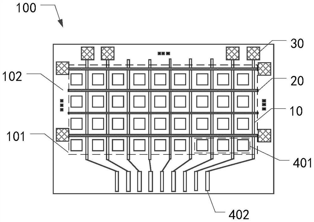
[0041] figure 1 A plan view of a display screen with an antistatic structure provided for an embodiment of the present application.
[0042] Such as figure 1As shown, this embodiment provides a display screen 100 with an antistatic structure, which includes a display area 101 and a non-display area 102 . Wherein, the display area 101 has a plurality of pixel units 401 arranged in an array, and each pixel unit 401 includes red sub-pixels, green sub-pixels and blue sub-pixels.
[0043] The display screen 100 includes a first metal wire 10 , a second metal wire 20 and a protection device 30 .
[0044] A plurality of first metal wires 10 are disposed in the display area 101 , and at least one end of each first metal wire 10 extends to the non-display area 102 .
[0045] A plurality of the second metal wires 20 are disposed in the display area 101 , and at least one end of each second metal wire 20 extends to the non-display area 102 .
[0046] A plurality of the protection dev...
Embodiment 2
[0073] This embodiment provides a display screen with an antistatic structure, including all the technical features of Embodiment 1, and at least one metal layer and an insulating layer.
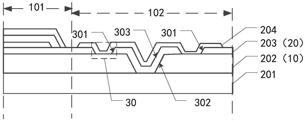
[0074] Figure 10 A cross-sectional view of a display screen with an antistatic structure provided for an embodiment of the present application.
[0075] Such as Figure 10 As shown, the display screen 100 located in the non-display area 102 includes a substrate 201 , a first metal layer 202 , a first insulating layer 203 , a second metal layer 204 , a second insulating layer 205 and a third metal layer 206 .
[0076] Specifically, the second insulating layer 205 is disposed on the top surface of the second metal layer 204 . The third metal layer 206 is disposed on the top surface of the second insulating layer 205 , and the third metal layer 206 is etched to form a third metal wire. The second insulating layer 205 includes a third through hole 304 penetrating to the top surface of the se...
PUM
 Abstract
Description
Claims
Application Information


