Array substrate as well as maintenance method and display device thereof

An array substrate and the same technology are applied in the fields of display devices, array substrates and maintenance methods thereof, which can solve the problems of prolonged production cycle, poor data line disconnection, poor gate line disconnection, etc., so as to ensure the success rate of maintenance and reduce production. The effect of cycle and operation method is simple and convenient

Inactive Publication Date: 2014-07-30
BOE TECH GRP CO LTD +1
View PDF5 Cites 3 Cited by
  • Summary
  • Abstract
  • Description
  • Claims
  • Application Information

AI Technical Summary

Problems solved by technology

In the actual manufacturing process of TFT-LCD, it is unavoidable that there will be poor grid line disconnection or data line disconnection. The commonly used maintenance method is to deposit metal at the disconnection for repair, but this method requires additional The deposition process will prolong the production cycle, and may even affect the aperture ratio of the display device, reducing the user's viewing effect

Method used


Image

  • Array substrate as well as maintenance method and display device thereof
  • Array substrate as well as maintenance method and display device thereof
  • Array substrate as well as maintenance method and display device thereof

Examples


Embodiment 1

[0034] An embodiment of the present invention provides an array substrate, such as figure 1 As shown, the array substrate includes:

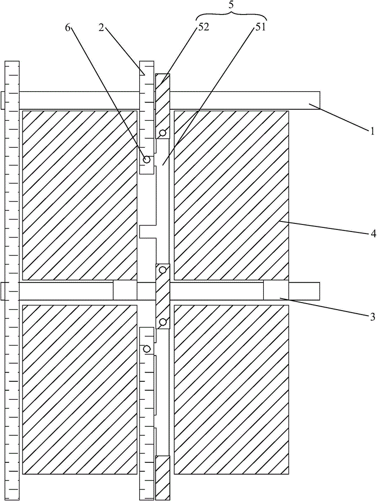
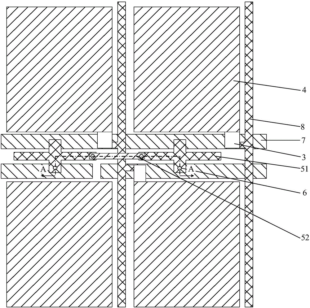
[0035] The first signal line 1 and the second signal line 2 formed on the array substrate, the first signal line 1 and the second signal line 2 intersect to define a plurality of pixel units, and each pixel unit includes a thin film transistor 3 and pixel electrode 4, further comprising:

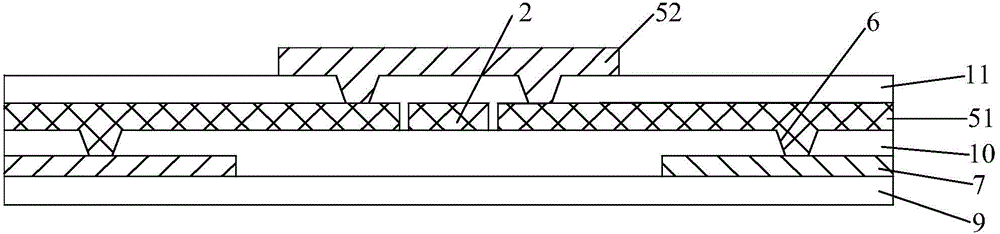
[0036] The connection structure 5 arranged side by side with the first signal line 1, wherein the connection structure 5 includes a first part 51 arranged on the same layer as the second signal line 2 and a first part 51 arranged on the same layer as the pixel electrode 4 Two parts 52, the first signal line 1, the second signal line 2 and the pixel electrode 4 are respectively in different layers, the first part 51 partially overlaps the first signal line 1, and the second part 52 Partially overlapping with the first portion 51 , the first portion 51 and the...

Embodiment 2

[0056] An embodiment of the present invention provides a method for maintaining the array substrate described in Embodiment 1, including:

[0057] If the first signal line is disconnected, the first part of the connection structure overlaps with the first signal line, and at the same time connects the first part and the second part of the connection structure overlaps.

[0058] Specifically, the overlap between the first part of the connection structure and the first signal line may be connected by welding, and the overlap between the first part and the second part of the connection structure may be connected by welding.

[0059] Among them, during welding, the laser can not only form a via hole connecting the first part and the first signal line at the intersection of the first part and the first signal line, but also use the instantaneous high temperature to melt the first part to fill it into the via hole , realizing the electrical connection between the first part and the ...


PUM


Abstract

The embodiment of the invention discloses an array substrate as well as a maintenance method and a display device thereof, relates to the technical field of display, which can maintain a broken wire by a simple and effective method and can ensure the maintenance success rate so that the production period is shortened and the yield of products is improved. The array substrate comprises a first signal wire and a second signal wire which are formed on the array substrate; the first signal wire and the second signal wire are crossed to define pixel units; each pixel unit comprises a thin film transistor and a pixel electrode; the array substrate further comprises a connection structure which is parallel to the first signal wire; the connection structure comprises a first part which is arranged on the same layer as the second signal wire and a second part which is arranged on the same layer as the pixel electrodes; the first signal wire, the second signal wire and the pixel electrodes are arranged on different layers; the first part and the first signal wire are partially overlapped; the second part and the first part are partially overlapped; the first part and the second part are arranged at an interval.

Description

technical field [0001] The present invention relates to the field of display technology, in particular to an array substrate, a maintenance method thereof, and a display device. Background technique [0002] Thin Film Transistor Liquid Crystal Display (TFT-LCD for short) has attracted much attention due to its small size, low power consumption, and no radiation. It occupies a dominant position in the field of flat panel display and is widely used in In all walks of life. In the actual manufacturing process of TFT-LCD, it is unavoidable that there will be poor grid line disconnection or data line disconnection. The commonly used maintenance method is to deposit metal at the disconnection for repair, but this method requires additional The deposition process will prolong the production cycle, and may even affect the aperture ratio of the display device, reducing the user's viewing effect. Contents of the invention [0003] The technical problem to be solved by the present ...

Claims


Application Information

Patent Timeline
Patent Type & Authority Applications(China)
IPC IPC(8): G02F1/1362G02F1/13H01L27/12
CPCG02F1/136259G02F1/136263
Inventor 陈曦毛国琪李梁梁刘耀
Owner BOE TECH GRP CO LTD
Why Eureka
Try Eureka