
Display panel and display device

A display panel and display pixel technology, applied in static indicators, nonlinear optics, optics, etc., can solve problems such as unpromoted, limited signal sources, immature technology, etc.

Active Publication Date: 2014-08-20
TCL CHINA STAR OPTOELECTRONICS TECH CO LTD
View PDF4 Cites 6 Cited by
  • Summary
  • Abstract
  • Description
  • Claims
  • Application Information

AI Technical Summary

Problems solved by technology

However, with the continuous development of new materials and technologies, the image quality gap between TFT-LCD and AMOLED is also narrowing, and due to immature technology and high production costs, AMOLED can only be used in small size
[0003] In addition, the resolution of the display panel is also increasing. Currently, the highest display resolution on the market has reached 3840*2160 (4K*2K) (that is, high-definition). Due to the limitation of the signal source, it has not been promoted yet.

Method used


Image

  • Display panel and display device
  • Display panel and display device
  • Display panel and display device

Examples


Embodiment Construction

[0042] The following descriptions of the various embodiments refer to the accompanying drawings to illustrate specific embodiments in which the present invention can be practiced. The directional terms mentioned in the present invention, such as "up", "down", "front", "back", "left", "right", "inside", "outside", "side", etc., are for reference only The orientation of the attached schema. Therefore, the directional terms used are used to illustrate and understand the present invention, but not to limit the present invention. In the figures, structurally similar units are denoted by the same reference numerals.

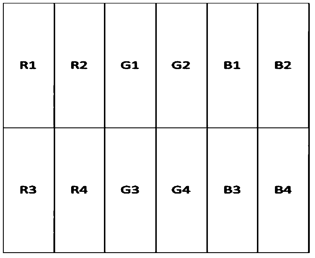
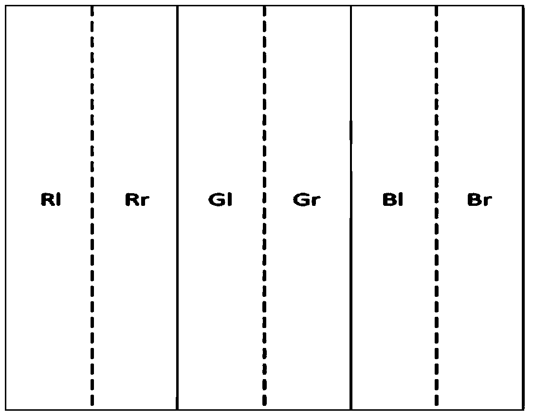
[0043] Please refer to figure 1 , a schematic diagram of the pixel unit structure of the first embodiment in the embodiment of the present invention.

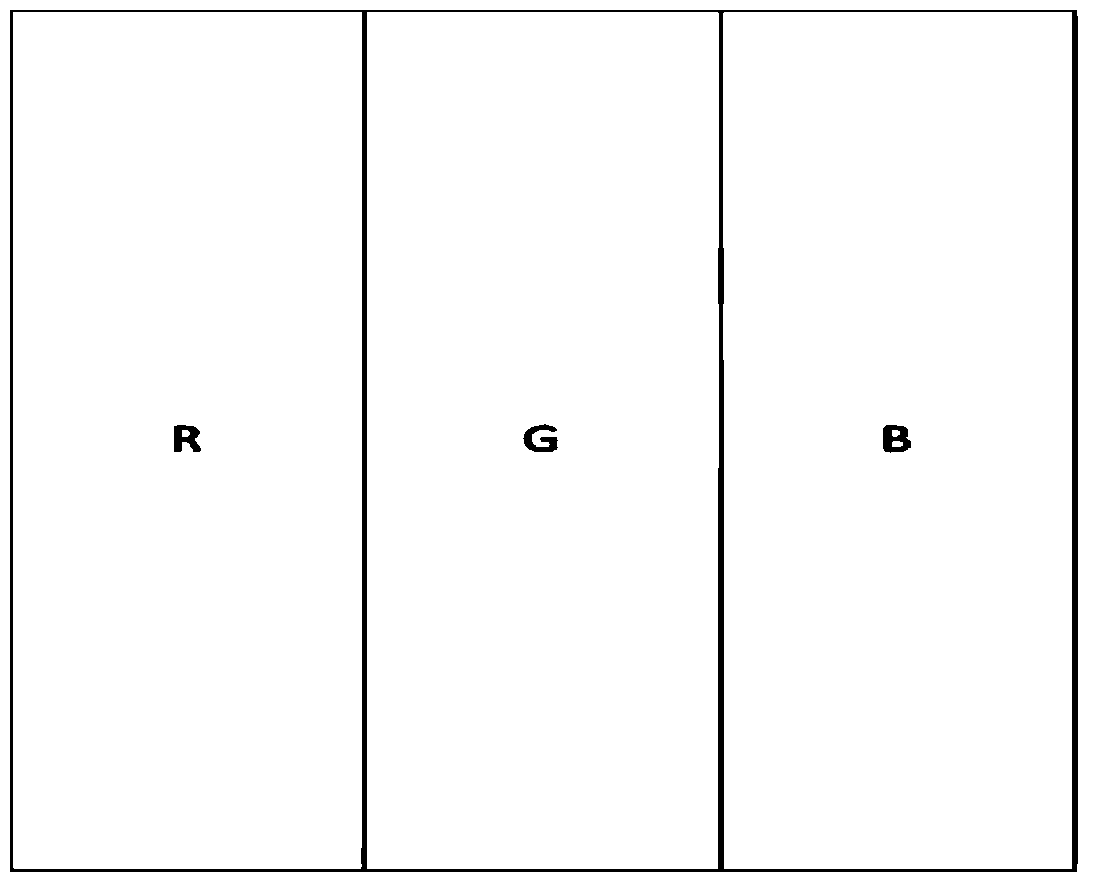
[0044] The display panel of the present invention includes an array substrate, the array substrate includes data lines, scan lines, and a plurality of pixel units formed by interlacing the data lines and the scan lin...


PUM


Abstract

The invention provides a display panel which comprises an array substrate. The array substrate comprises a data line, a scan line and multiple pixel units formed by the data line and the scan line in a staggered mode. Each pixel unit comprises at least two pixel subunits. Each subunit comprises a blue sub-pixel, a red sub-pixel and a green sub-pixel, the blue sub-pixels in the same pixel unit are adjacent, the red sub-pixels in the same pixel unit are adjacent, and the green sub-pixels in the same pixel unit are adjacent. The display panel can be automatically switched between 2D images and 3D images, the images are smoother, and production cost is reduced.

Description

【Technical field】 [0001] The present invention relates to the field of display technology, in particular to a display panel and a display device. 【Background technique】 [0002] The current mainstream display panels include: TFT-LCD (Thin Film Transistor Liquid Crystal Display) and AMOLED (Active Matrix Organic Light Emitting Diode Display Panel). As a new generation of display technology, AMOLED has its unique display advantages, such as a wider color gamut. Wider, faster response, better brightness, wider viewing angle, lower power consumption, smaller size, etc. However, with the continuous development of new materials and technologies, the image quality gap between TFT-LCD and AMOLED is also shrinking, and due to immature technology and high production costs, AMOLED can only be used in small size. [0003] In addition, the resolution of the display panel is also continuously increasing. Currently, the highest display resolution on the market has reached 3840*2160 (4K*2...

Claims


Application Information

Patent Timeline
Patent Type & Authority Applications(China)
IPC IPC(8): G02F1/133G02F1/1362
CPCG09G3/003G09G3/3225G09G3/3648G09G3/3666G09G2300/0452G09G2310/0205G09G2310/0281G09G2310/08G09G2320/0613G09G2320/08
Inventor 徐向阳
Owner TCL CHINA STAR OPTOELECTRONICS TECH CO LTD
Learn More