Pixel driving circuit and driving method thereof as well as display device

A technology of a pixel driving circuit and a driving method, which is applied to static indicators, instruments, etc., can solve problems such as inconsistencies, brightness differences of display devices, and influence on screen display effects, etc., to offset operating currents, solve threshold voltage inconsistencies, and improve screen display effect of effect

Active Publication Date: 2014-09-10
BOE TECH GRP CO LTD +1
View PDF6 Cites 28 Cited by
  • Summary
  • Abstract
  • Description
  • Claims
  • Application Information

AI Technical Summary

Problems solved by technology

The threshold voltage V th Will drift, resulting in the current flowing through the organic light-emitting diode OLED of each pixel (ie, the operating current I OLED ) due to the threshold voltage V th The drift becomes inconsistent, and the brightness of each pixel of the display device is different, which ultimately affects the display effect of the entire screen

Method used


Image

  • Pixel driving circuit and driving method thereof as well as display device
  • Pixel driving circuit and driving method thereof as well as display device
  • Pixel driving circuit and driving method thereof as well as display device

Examples


Embodiment 1

[0035] This embodiment provides a pixel driving circuit, including: a driving transistor and an organic light emitting diode connected to the driving transistor. The pixel driving circuit further includes: a first switching tube connected to the driving transistor, and the first switching tube is controlled by the first A scanning signal connected to the power supply voltage; a storage capacitor connected to the driving transistor; a second switching tube connected to the storage capacitor, the second switching tube is controlled by the second scanning signal and connected to the data voltage; connected to the driving transistor and the third switch tube between the common end of the first switch tube and the common end of the drive transistor and the storage capacitor, the third switch tube is controlled by the third scan signal; the third switch tube connected to the common end of the drive transistor and the organic light emitting diode Four switch tubes, the fourth switch t...

Embodiment 2

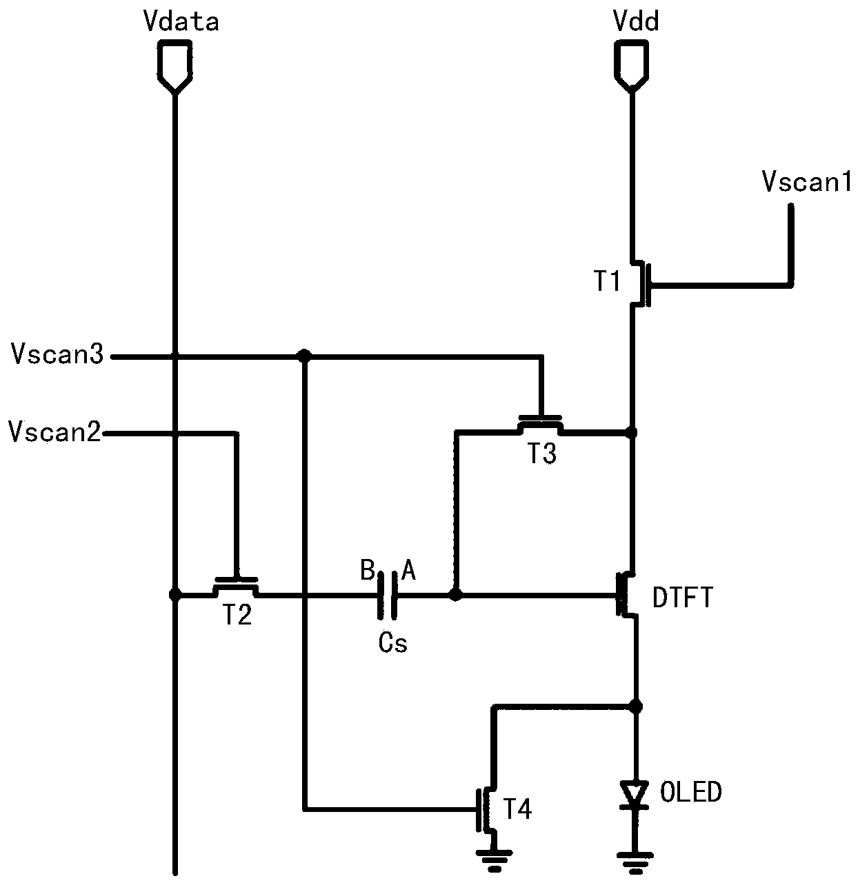
[0039] Based on Embodiment 1, this embodiment specifically provides a pixel driving circuit, such as figure 2 As shown, the circuit includes: an organic light emitting diode OLED, a driving transistor DTFT, a first switching tube T1, a second switching tube T2, a third switching tube T3, a fourth switching tube T4 and a storage capacitor Cs.

[0040] The connection relationship between the above components is the same as that of the pixel driving circuit described in Embodiment 1, and the more specific connection relationship can preferably be as follows:

[0041] The organic light emitting diode OLED is connected with the output terminal of the driving transistor DTFT.

[0042] The control end of the first switching tube T1 is connected to the first scanning signal Vscan1, the input end is connected to the power supply voltage Vdd, and the output end is connected to the input end of the driving transistor DTFT.

[0043] The control end of the second switching transistor T2 ...

Embodiment 3

[0076] When the types of the first switch tube and the second switch tube are different, the first scan signal and the second scan signal are the same, and the first switch tube and the second switch tube can preferably be connected to the same scan line. Based on this, this embodiment provides a pixel driving circuit, the structure of which is as follows Figure 8 As shown, the first switching transistor T1 and the second switching transistor T2 are connected to the same scanning line and controlled by the same scanning signal. At this time, the type of the first switching transistor T1 may be N-type, and the type of the second switching transistor is P-type; or the type of the first switching transistor T1 may be P-type, and the type of the second switching transistor is N-type.

[0077] The driving method of the pixel driving circuit provided in this embodiment is the same as the driving method introduced in the first embodiment, and will not be repeated here.

[0078] If ...


PUM


Abstract

The invention provides a pixel driving circuit and a driving method thereof as well as a display device. The pixel driving circuit comprises a driving transistor, first to fourth switching tubes and a storage capacitor. The driving method comprises the following steps: charging the storage capacitor; discharging the storage capacitor in order to generate a voltage difference between the voltages at the two ends of the storage capacitor; changing the data voltage in order to generate the same changes of the voltages at the two ends of the storage capacitor as the data voltage; driving an organic light-emitting diode to emit light. By adopting the driving circuit and the driving method, compensation of the threshold voltage of driving voltage for driving a transistor is realized, the influence of the threshold voltage on the working current of the organic light-emitting diode is counteracted, the problem of non-uniform brightness of pixel points due to inconsistent threshold voltage for driving the transistor at different pixel points is solved completely, and the picture display effect of the display device is improved.

Description

technical field [0001] The present invention relates to the field of display technology, in particular to a pixel driving circuit, a driving method thereof, and a display device. Background technique [0002] With the continuous development of display technology, OLED (Organic Light-Emitting Diode, Organic Light-Emitting Diode) display device has become a popular choice due to its advantages such as simple manufacturing process, lighter and thinner products, high luminous brightness, fast response speed, low cost, and low operating temperature. One of the current mainstream display technologies. [0003] According to different driving methods, OLED display devices can be divided into two types: PMOLED (Passive Matrix Organic Light Emission Display, passive matrix organic light emitting diode display device) and AMOLED (Active Matrix Organic Light Emission Display, active matrix organic light emitting diode display device). kind. Compared with PMOLED, AMOLED has a faster re...

Claims


Application Information

Patent Timeline
Patent Type & Authority Applications(China)
IPC IPC(8): G09G3/32G09G3/3233G09G3/3258
CPCG09G2300/0819G09G2300/0842G09G2300/0861G09G2320/045G09G3/3233G09G3/3258G09G2310/0251G09G2320/0233
Inventor 杨盛际
Owner BOE TECH GRP CO LTD
Why Eureka
Try Eureka