Solar cell module back sheet, method for manufacturing solar cell module back sheet, and solar cell module
A technology of solar cells and manufacturing methods, applied in the direction of electrical components, chemical instruments and methods, applications, etc., can solve the problems of increased cost, high price, damage to the original backplane for black solar cell modules, etc., and achieve difficult discoloration and inhibition The effect of the increase in cost
- Summary
- Abstract
- Description
- Claims
- Application Information
AI Technical Summary
Problems solved by technology
Method used
Image
Examples
Embodiment approach
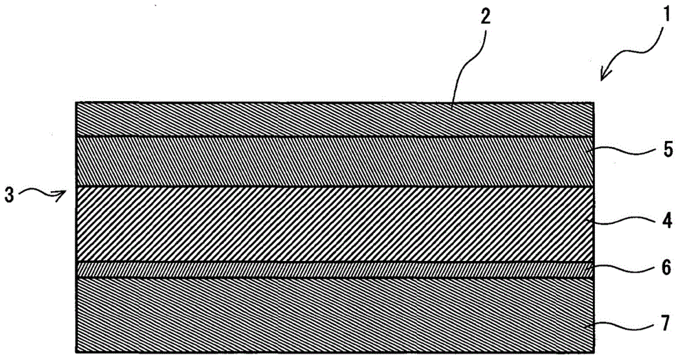
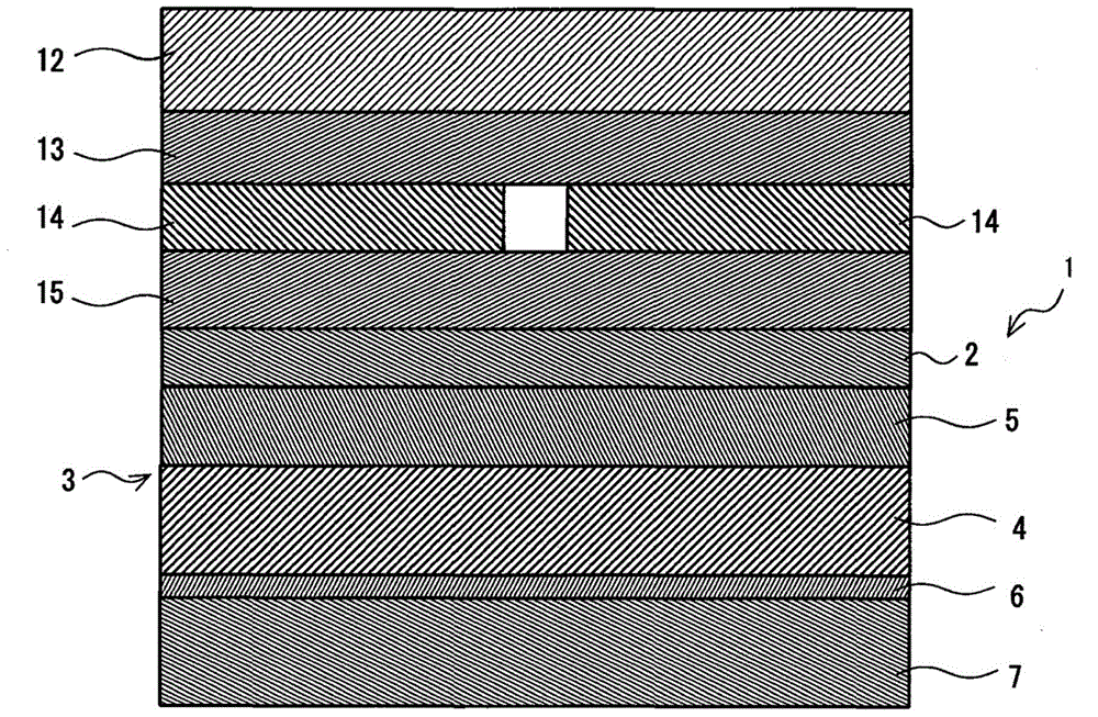
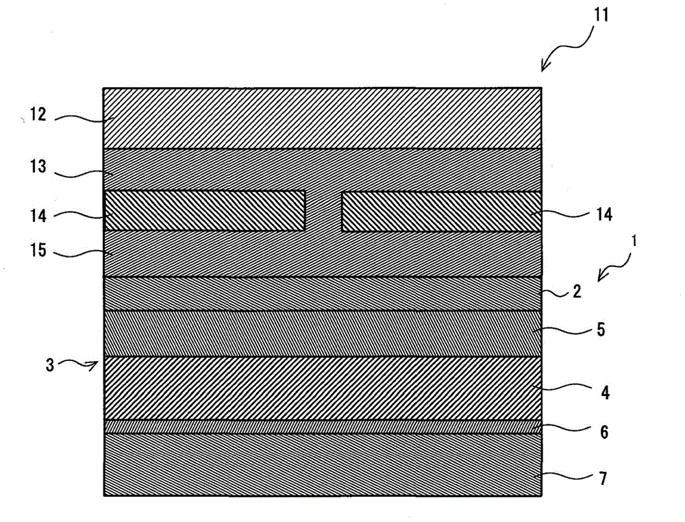
[0156] In addition, the present invention is not limited to the structures of the embodiments. That is, in the above-mentioned embodiment, the mode in which the colored layer 2 is provided on the outermost surface has been described, but the present invention is not limited thereto. For example, a transparent or translucent layer may be provided on the surface of the colored layer 2 in the above-mentioned embodiment. hot melt adhesive layer.
[0157] In addition, in the said embodiment, the base material sheet 3 was demonstrated as white, but this invention is not limited to this, For example, you may make the base material sheet 3 transparent or translucent. Also in this case, the colored layer 2 may be laminated on the back side of the base sheet 3 .
[0158] In addition, even when the base sheet 3 is made white, it is not limited to the form of providing the white layer 5 as shown in the above-mentioned embodiment, and the design may be appropriately changed, and a white s...
Embodiment 1
[0165] The test results of the invention will be specifically described below through examples, but the invention is not limited to the following examples.
[0166]
[0167] The reflectance when the colored layer 2 of the back sheet 1 was formed by applying the coating liquid on the surface of the base material sheet 3 (white layer 5 ) was measured.
[0168] As the base sheet 3, a polyethylene film (W-PO (white) manufactured by Kewa Co., Ltd.) with a thickness of 110 μm was used as the white layer 5, and a polyester film with a thickness of 188 μm (S10 (transparent) manufactured by Toray Co., Ltd.) was used. A film laminated with a polytetrafluoroethylene film (25PWA manufactured by Asahi Glass Co., Ltd.) having a thickness of 25 μm was used as the base film 4 .
[0169] In addition, a red pigment (Ramic SR915R red manufactured by Dainichi Seika Co., Ltd.) with a concentration of 27% was used at a mixing ratio of 34.9%, and a blue pigment with a concentration of 27% (Ramic S...
PUM
| Property | Measurement | Unit |
|---|---|---|
| thickness | aaaaa | aaaaa |
| surface roughness | aaaaa | aaaaa |
| particle size | aaaaa | aaaaa |
Abstract
Description
Claims
Application Information
 - R&D
- Intellectual Property
- Life Sciences
- Materials
- Tech Scout
- Unparalleled Data Quality
- Higher Quality Content
- 60% Fewer Hallucinations
Browse by: Latest US Patents, China's latest patents, Technical Efficacy Thesaurus, Application Domain, Technology Topic, Popular Technical Reports.
© 2025 PatSnap. All rights reserved.Legal|Privacy policy|Modern Slavery Act Transparency Statement|Sitemap|About US| Contact US: help@patsnap.com


