Integrated inductor structure and method for manufacturing integrated inductor structure

A technology of integrated inductance and manufacturing method, which is applied in the field of integrated inductance structure manufacturing, can solve the problems of poor blocking effect and inability to effectively reduce eddy current, and achieve the effect of complete blocking effect and improved quality factor

Active Publication Date: 2018-02-06
REALTEK SEMICON CORP
View PDF5 Cites 0 Cited by
  • Summary
  • Abstract
  • Description
  • Claims
  • Application Information

AI Technical Summary

Problems solved by technology

like figure 1 As shown, the patterned ground guard 22 is formed between the inductor 30 and the gate oxide layer 24, however, such a patterned ground guard 22 has a poor blocking effect on the eddy current formed in the deep layer of the semiconductor substrate 10, and figure 1 The material of the patterned ground protection 22 is polysilicon, which cannot effectively reduce the eddy current

Method used


Image

  • Integrated inductor structure and method for manufacturing integrated inductor structure
  • Integrated inductor structure and method for manufacturing integrated inductor structure
  • Integrated inductor structure and method for manufacturing integrated inductor structure

Examples


no. 1 example

[0066] Please refer to Figure 4 , Figure 4 What is shown is a flowchart of a first embodiment of the method for manufacturing an integrated inductor structure of the present invention based on the aforementioned integrated inductor structure 200. If substantially the same result can be obtained, the steps in the process do not necessarily need to be followed. Figure 4 The sequence shown does not necessarily need to be sequential, that is, other steps may be inserted between these steps. The first embodiment of the method for manufacturing an integrated inductor structure of the present invention includes the following steps:

[0067] Step 400: Form a semiconductor substrate.

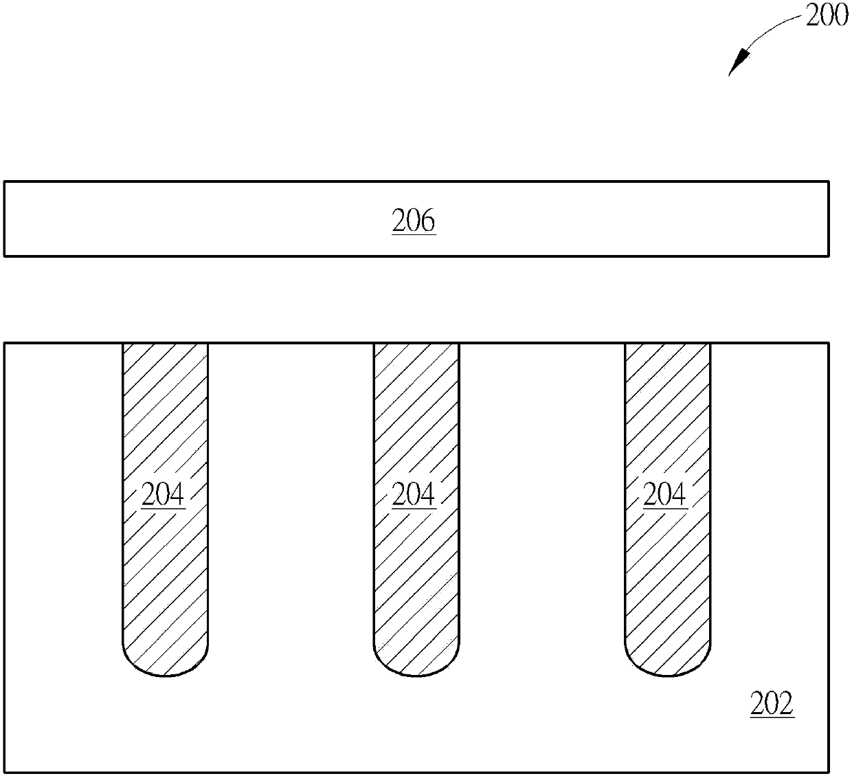
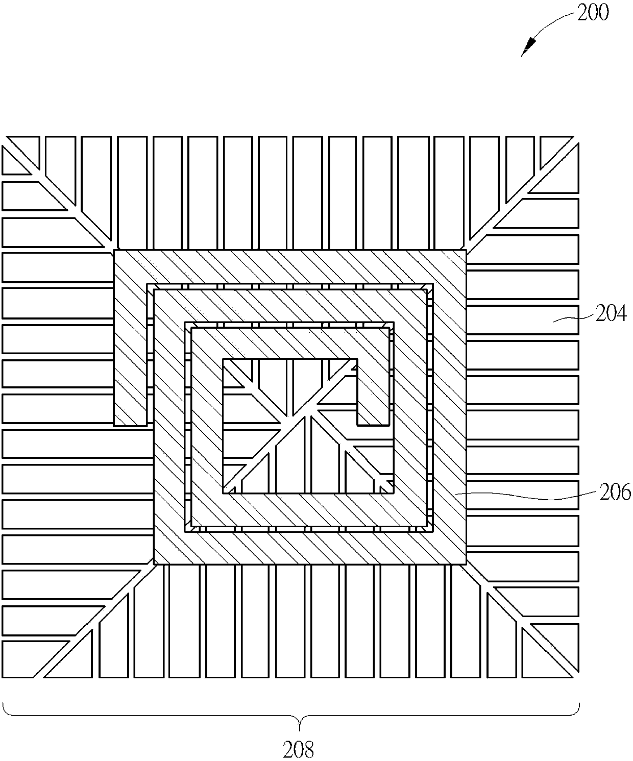
[0068] Step 402: Form a plurality of deep trenches in the semiconductor substrate, and arrange the plurality of deep trenches into a specific pattern.

[0069] Step 404 : Fill a metal material in the plurality of deep trenches to form a patterned ground shield.

[0070] Step 406 : Form an inductor...

no. 4 example

[0081] Please refer to Figure 13 , Figure 13 What is shown is a flowchart of a fourth embodiment of the integrated inductor structure manufacturing method of the present invention based on the above-mentioned integrated inductor structure 700. If substantially the same result can be obtained, the steps in the process do not necessarily need to be followed. Figure 13 The sequence shown does not necessarily need to be sequential, that is, other steps may be inserted between these steps. The fourth embodiment of the integrated inductor structure manufacturing method of the present invention includes the following steps:

[0082] Step 800: Form a semiconductor substrate.

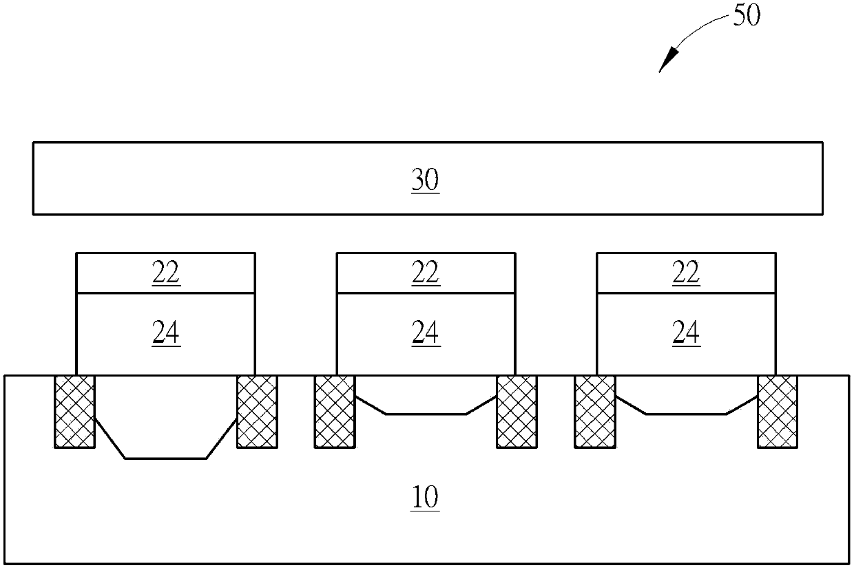
[0083] Step 802: Form an inductor over the semiconductor substrate.

[0084] Step 804 : Form a redistributed metal layer with a specific pattern on the inductor to form a patterned ground shield.

[0085] Please note that the above-mentioned embodiments are only used as illustrations of the present invent...


PUM


Abstract

The invention discloses an integrated inductor structure and an integrated inductor structure fabrication method. The integrated inductor structure comprises a semiconductor substrate, a plurality of deep trenches and an inductor, wherein the plurality of deep trenches are formed in the semiconductor substrate and arranged in a specific pattern, a metal material is filled in the plurality of deep trenches to form patterned grounding protection; and the inductor is formed above the semiconductor substrate. The integrated inductor structure fabrication method comprises the following steps of: forming the semiconductor substrate; forming the plurality of deep trenches in the semiconductor substrate and arranging the plurality of deep trenches in the specific pattern; filling the metal material in the plurality of deep trenches to form the patterned grounding protection; and forming the inductor above the semiconductor substrate.

Description

technical field [0001] The present invention relates to an integrated inductance structure and a method for manufacturing the integrated inductance structure, in particular to an integrated inductance structure with an innovative patterned ground shield (Patterned Ground Shield, PGS) and a method for manufacturing the integrated inductance structure . Background technique [0002] With the development of IC manufacturing System-on-a-Chip (SoC), passive components such as integrated inductors have been widely integrated into high-frequency integrated circuits. Since IC manufacturing generally adopts a silicon substrate structure, integrated inductors have a low quality factor (Q-factor) problem due to substrate loss. [0003] Therefore, it has been proposed to use a patterned ground shield (PGS) made of polysilicon (polysilicon) metal to reduce the eddy current (eddy current) of the integrated inductor to improve the quality factor. For example, please refer to figure 1 , ...

Claims


Application Information

Patent Timeline
Patent Type & Authority Patents(China)
IPC IPC(8): H01L23/64H01L23/58H01L21/02
CPCH01L2224/16225
Inventor 叶达勋
Owner REALTEK SEMICON CORP
Why Eureka
Try Eureka