

Organic light-emitting display panel and manufacturing method thereof
A technology of light-emitting display and organic light-emitting layer, which is applied in semiconductor/solid-state device manufacturing, semiconductor devices, electrical components, etc. The effect of small color shift
- Summary
- Abstract
- Description
- Claims
- Application Information
AI Technical Summary
Problems solved by technology
Method used
Image

Examples
Embodiment Construction
[0022] The present invention will be further described in detail below in conjunction with the accompanying drawings and embodiments. It should be understood that the specific embodiments described here are only used to explain the present invention, but not to limit the present invention. In addition, it should be noted that, for the convenience of description, only some structures related to the present invention are shown in the drawings but not all structures.
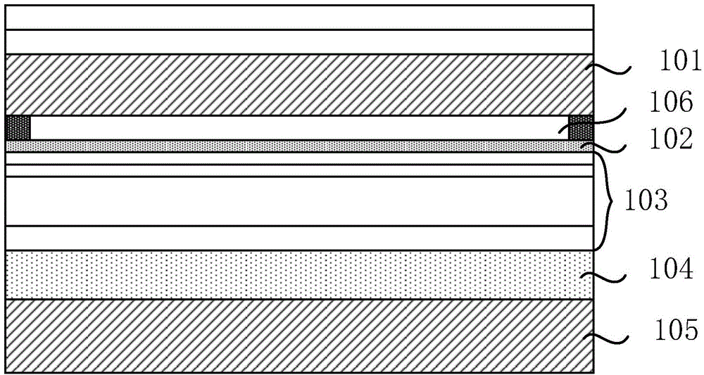
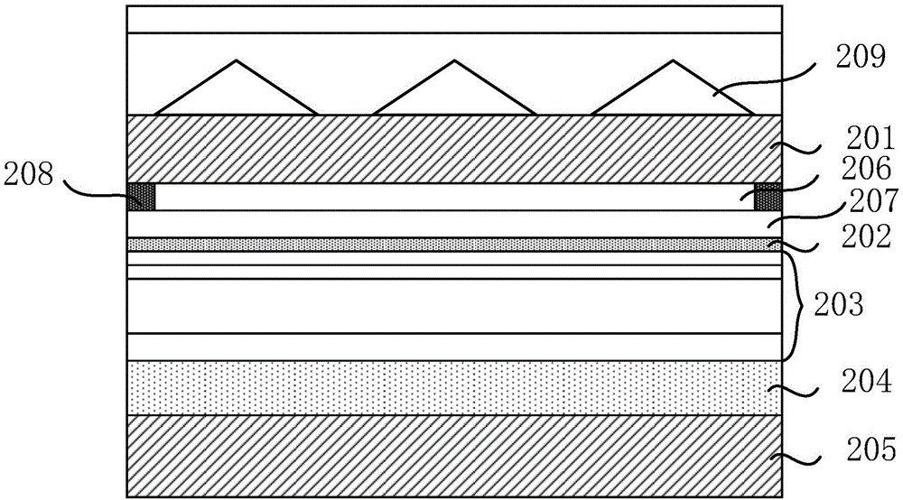
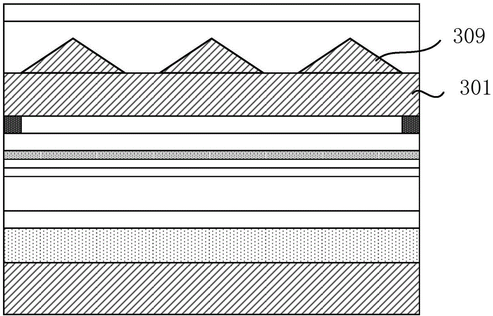
[0023] An embodiment of the present invention provides an organic light-emitting display panel, including an upper substrate, a first electrode layer, an organic light-emitting layer, a second electrode layer, and a lower substrate arranged in sequence, wherein the first electrode layer faces away from the organic A refraction layer is provided on one side of the luminous layer, and the refraction layer includes a plurality of convex bodies, the convex bodies have sharp corners, and the sharp corners face to the si...
PUM
| Property | Measurement | Unit |
|---|---|---|
| Base radius | aaaaa | aaaaa |
Abstract
Description
Claims
Application Information