
Compiling method and device for memory

A memory and buffer technology, applied in the electronic field, can solve the problems of wasting verify and program time, and achieve the effects of improving efficiency, reducing time, and saving time

Active Publication Date: 2014-10-15
GIGADEVICE SEMICON (BEIJING) INC
View PDF4 Cites 0 Cited by
  • Summary
  • Abstract
  • Description
  • Claims
  • Application Information

AI Technical Summary

Problems solved by technology

The disadvantage is that writing data to multiple consecutive addresses will repeat the operation of multiple single addresses, wasting a lot of verify and program time

Method used


Image

  • Compiling method and device for memory
  • Compiling method and device for memory

Examples


Embodiment 1

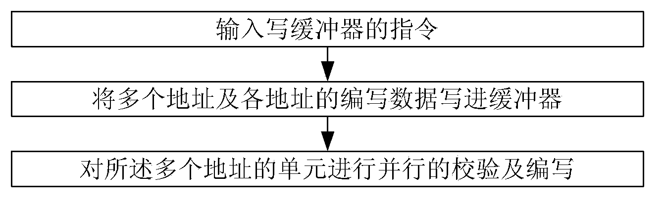
[0030] Embodiment 1, a method for writing a memory, such as figure 2 shown, including:

[0031] Input the command to write the buffer to clear the data in the buffer;

[0032] Write the addresses of N units in the memory and the programming data corresponding to each address into the buffer; wherein, N is a positive integer;

[0033] Perform verification and programming on the N units in parallel according to the writing data in the buffer; wherein, writing to any unit means: writing the writing data corresponding to the address of the unit in the buffer into the unit.

[0034] In an implementation manner of this embodiment, N is 64 or 128.

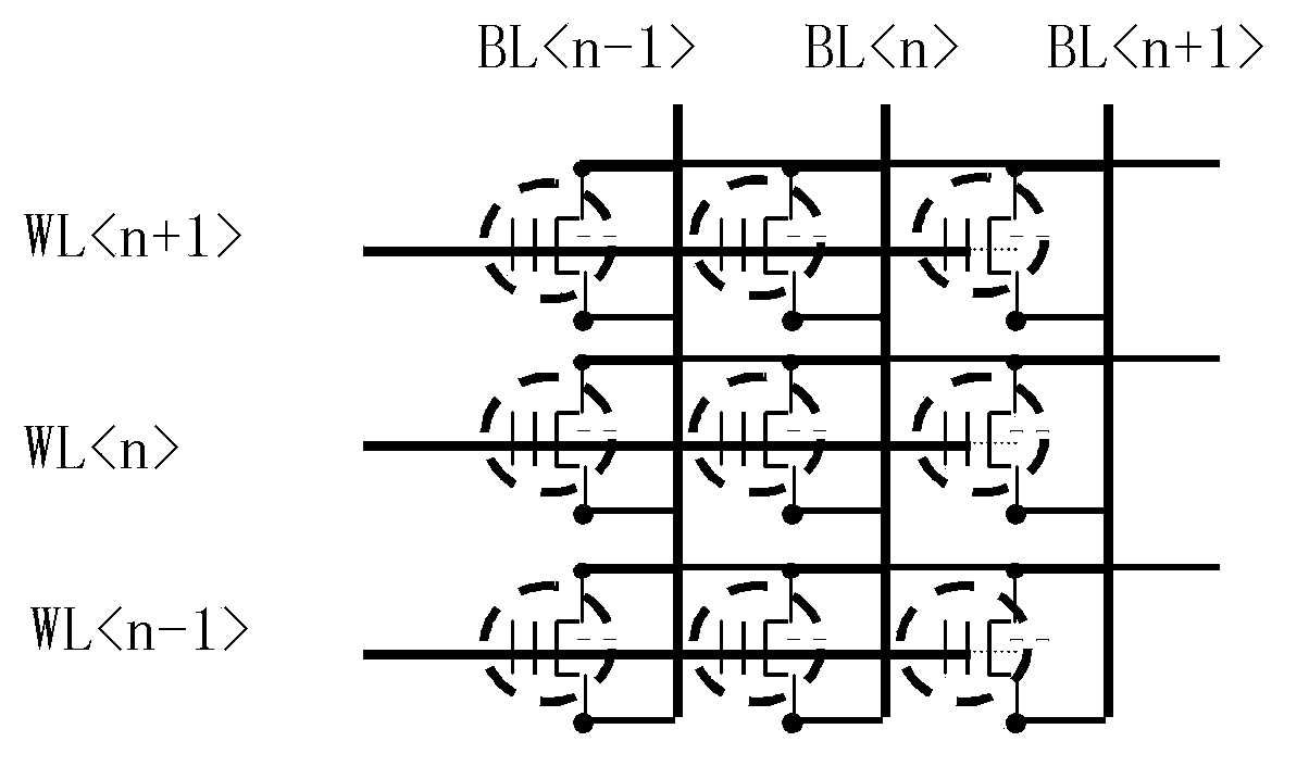
[0035] This embodiment can write 64bits or 128bits data at one time; taking the situation when writing 128bit data as an example, the circuit is changed from the original word line connecting 8 or 16 bit lines to one word line connecting 128 bits Wire. If the drive capability (strength) of the pump is not enough to supp...

Embodiment 2

[0060] Embodiment 2. A device for writing a memory, comprising:

[0061] buffer;

[0062] The control unit is used to input an instruction for writing the buffer, and clear the data in the buffer; and write the addresses of the N units in the memory and the writing data corresponding to each address into the buffer; N is a positive integer;

[0063] A writing unit, configured to verify and write the N units in parallel according to the writing data in the buffer; wherein, writing any one unit refers to: writing the address of the unit in the buffer Write data is written to the unit.

[0064] In an implementation manner of this embodiment, N is 64 or 128.

[0065] In an implementation manner of this embodiment, the control unit can also be used to reload the one or more addresses if it is judged that the data in one or more addresses has an error before inputting the command to write the buffer. , and writing data of the one or more addresses to the buffer; input...


PUM


Abstract

The invention provides a compiling method and a compiling device for a memory. The method comprises the following steps that a buffer writing instruction is input, and data in a buffer is subjected to zero clearing; addresses of N units in the memory and compiling data corresponding to each address are written into the buffer, wherein N is a positive integer; the N units are parallelly checked and compiled according to the compiling data in the buffer, wherein the compiling on any one unit refers to the operation of writing the compiling data corresponding to the unit in the buffer into the unit. The method and the device have the advantage that the compiling speed of the memory can be accelerated.

Description

technical field [0001] The present invention relates to the field of electronics, in particular to a memory writing method and device. Background technique [0002] With the rapid development of various electronic technologies and the rapid expansion of the electronic market, the demand for memory is growing rapidly. Among many memory types, NOR flash memory is widely used in various electronic devices, such as mobile products, automotive electronics, etc., due to its fast random read and write speed and high reliability. Since its development in 1988, NOR-type flash memory technology has been continuously improved and updated in line with market development needs. Not only has the capacity increased day by day, but also its reliability has become higher and higher, and the random read and write speed has also become faster and faster. [0003] For a memory, each unit cell corresponds to a word line and a bit line. If you want to program (write) a cell, you need to add a h...

Claims


Application Information

Patent Timeline
IPC IPC(8): G06F12/08G06F3/06G06F12/0891
Inventor 苏志强潘荣华崔茂兴
Owner GIGADEVICE SEMICON (BEIJING) INC
Features
  • Generate Ideas
  • Intellectual Property
  • Life Sciences
  • Materials
  • Tech Scout
  • Unparalleled Data Quality
  • Higher Quality Content
  • 60% Fewer Hallucinations
Learn More