


Quick Research
Generate reliable direction feasibility study reports for your R&D in just a few steps.

Technical Q&A
Discover and master advanced knowledge NOW. Basics, ideas, possibilities, all at once.

Find Solutions
As an expert in R&D theories, this can generate solutions to your technical problems instantly.

Evaluate Feasibility
Analyze your overall solution with one click, know your potential R&D risks in advance.

Monitor Landscape
Get weekly tech updates, stay abreast of the latest tech innovations and key insights.
A method for mechanically processing complex nanostructures in the same scribing direction of an AFM probe
A directional mechanical and nano-structure technology, applied in the direction of micro-structure technology, micro-structure device, manufacturing micro-structure device, etc., can solve the problems of inconsistent processing structure depth and processing quality, and achieve good processing quality consistency, simple processing method, Simple to use effects
- Summary
- Abstract
- Description
- Claims
- Application Information
AI Technical Summary
Problems solved by technology
Method used
Image

Examples
specific Embodiment approach 1
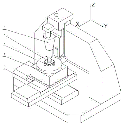
[0019] Specific implementation mode one: as figure 1 As shown, a device for mechanically processing complex nanostructures in the same scribing direction provided by an AFM probe in this embodiment includes: AFM (Q-Scope250; Ambios Company, USA) 1, a processed sample 2, a manual two-dimensional adjustment table ( Sigma, Japan)3, precision spindle (ABRS-150MP, Aerotech, USA)4 and two-dimensional high-precision positioning platform (M511.HD; PICompany, Germany)5. In the picture, the processed sample 2 is fixed on the manual two-dimensional adjustment table 3, the bottom of the manual two-dimensional adjustment table 3 is connected to the upper end of the precision spindle 4, and the lower end of the precision spindle 4 is connected to the two-dimensional high-precision positioning platform 5, two-dimensional The base of the high precision positioning platform 5 is fixedly connected on the sample stage of AFM1. Both the precision spindle 4 and the two-dimensional high-precision ...
specific Embodiment approach 2
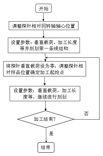
[0022] Specific embodiment 2: This embodiment provides a method for mechanically processing complex nanostructures in the same scribing direction of an AFM probe, including the following steps:
[0023] 1. First, carry out rough centering on the precision spindle, and roughly determine the relative position of the AFM probe and the center of rotation of the precision spindle; then apply a certain load to the AFM probe and keep it still, control the precision spindle to rotate 360°, use the AFM The three-dimensional topography detection function obtains the surface topography map after nano-processing, and obtains the rotation center of the precision spindle by extracting the circular trajectory image of the surface topography map, so as to realize the precise comparison between the contact point of the AFM probe and the sample surface and the center of rotation Location.
[0024] 2. Determine the processing and scoring position of the AFM needle tip, and control the position m...
specific Embodiment approach 3
[0027] Specific implementation mode three: as figure 2 As shown, this embodiment provides a method for mechanically processing complex nanostructures in the same scribing direction of the AFM probe, and the specific steps are as follows:
[0028] Step 1: Align the center and determine the relative position of the AFM probe press-in position and the center of rotation of the precision spindle; it is divided into two methods: coarse alignment and fine alignment.
[0029] (1) Coarse centering
[0030] The processed sample is fixed on the manual two-dimensional adjustment table, and a cross-shaped mark is made on the surface of the processed sample. Through observation under an optical microscope, the manual two-dimensional adjustment table is used to roughly adjust the center of the cross-shaped mark to the precision spindle rotation center location nearby. At this time, the AFM probe is close to the sample surface, and the AFM auxiliary optical microscope is used to clearly s...
PUM
 Abstract
Description
Claims
Application Information
 - R&D Engineer
- R&D Manager
- IP Professional
- Industry Leading Data Capabilities
- Powerful AI technology
- Patent DNA Extraction
Browse by: Latest US Patents, China's latest patents, Technical Efficacy Thesaurus, Application Domain, Technology Topic, Popular Technical Reports.
© 2024 PatSnap. All rights reserved.Legal|Privacy policy|Modern Slavery Act Transparency Statement|Sitemap|About US| Contact US: help@patsnap.com