Touch display device and manufacturing method thereof

A technology of a touch display device and a manufacturing method, which are applied in the fields of optics, instruments, electrical digital data processing, etc., can solve the problems of specular reflection, affecting the display quality of the touch display device 20, etc., so as to avoid specular reflection, improve display quality, Avoid the effect of interference fringes

Active Publication Date: 2014-12-10
KUSN INFOVISION OPTOELECTRONICS
View PDF7 Cites 21 Cited by
  • Summary
  • Abstract
  • Description
  • Claims
  • Application Information

AI Technical Summary

Problems solved by technology

However, since the touch sensing layer 25 is made of metal conductive material and generally has a relatively flat surface 25a, when the light is incident on the touch sensing layer 25, there will be a mirror reflection phenomenon, causing the viewer to watch the touch sensing layer 25 from certain angles. When the touch display device 20 is controlled, there will be bright and dark areas at intervals, and there will be interference fringes of light and dark, which will affect the display quality of the touch display device 20

Method used


Image

  • Touch display device and manufacturing method thereof
  • Touch display device and manufacturing method thereof
  • Touch display device and manufacturing method thereof

Examples


Embodiment Construction

[0033] In order to further explain the technical means and effects adopted by the present invention to achieve the intended invention purpose, the specific implementation, structure, The features and their functions are detailed as follows:

[0034] The aforementioned and other technical contents, features and effects of the present invention will be clearly presented in the following detailed description of preferred embodiments with reference to the drawings. Through the description of specific implementation methods, the technical means and effects of the present invention to achieve the intended purpose can be understood more deeply and specifically, but the attached drawings are only for reference and description, and are not used to explain the present invention limit.

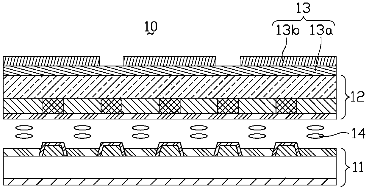
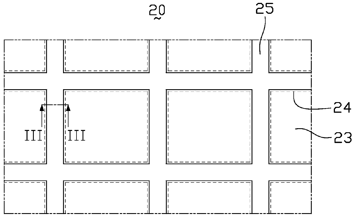
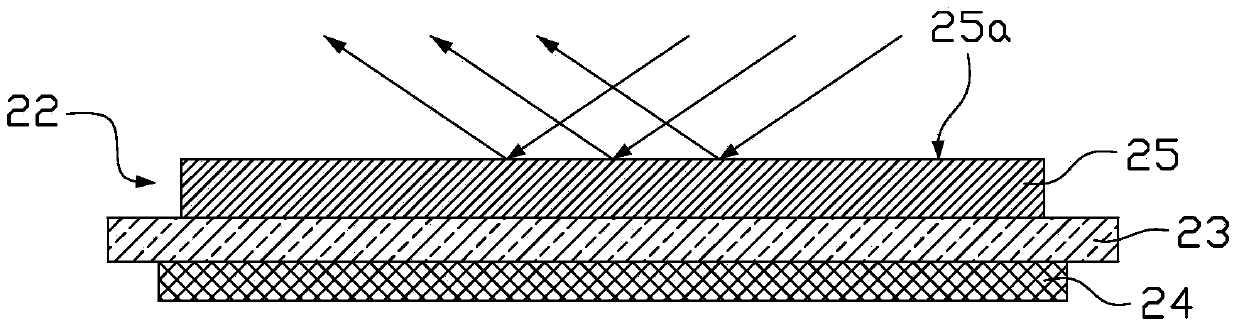
[0035] Figure 4 It is a partial top structural schematic diagram of the touch display device according to the first embodiment of the present invention. Figure 5 is along Figure 4 Sectional view o...


PUM

PropertyMeasurementUnit
refractive indexaaaaaaaaaa

Abstract

The invention discloses a touch display device which comprises a display substrate, a transparent concave-convex structural layer and a touch sensing layer. The display substrate comprises an array substrate, a colored filtering substrate and a liquid crystal layer clamped between the array substrate and the colored filtering substrate. The colored filtering substrate is located above the array substrate and is provided with a first surface opposite to the array substrate and a second surface away from the array substrate and opposite to the first surface. The colored filtering substrate comprises a black matrix layer arranged on the first surface. The transparent concave-convex structural layer is arranged on the second surface of the colored filtering substrate and provided with a first concave-convex surface. The touch sensing layer is located on the side, provided with the transparent concave-convex structural layer, of the colored filtering substrate. The projection of the edge of the touch sensing layer on the colored filtering substrate is within the range of the projection of the black matrix layer on the colored filtering substrate. The touch display device has the high penetration rate, can effectively eliminate the specular reflection phenomenon of the touch sensing layer, and is beneficial to improving display quality. The invention further relates to a manufacturing method of the touch display device.

Description

technical field [0001] The present invention relates to the technical field of touch display, and in particular to a touch display device and a manufacturing method thereof. Background technique [0002] The touch technologies of the existing touch display devices mainly include plug-in, one glass solution (OGS), in-cell and on-cell technologies. Since the touch screen and the display panel are set independently of each other, the plug-in touch display device has a large thickness and cannot meet the ultra-thin requirements of some handheld devices and portable devices, and has been gradually eliminated. The touch display device of OGS integrates the touch sensing layer and the protective glass and then attaches it to the display panel through optical glue. It has the advantages of high touch sensitivity and is one of the current mainstream touch technologies. The main disadvantages It is not strong enough and fragile. In Cell's touch display device integrates the touch se...

Claims


Application Information

Patent Timeline
Patent Type & Authority Applications(China)
IPC IPC(8): G06F3/041G02F1/1333
Inventor 钟德镇李雪红唐先柱
Owner KUSN INFOVISION OPTOELECTRONICS
Why Eureka
Try Eureka