Touch panel and display device
A touch panel and substrate technology, which is applied in the fields of instruments, electrical digital data processing, digital data processing components, etc., can solve the problems of complex structure and manufacturing process of touch panels, and is conducive to thinning, simplifying structure and manufacturing process. Effect
- Summary
- Abstract
- Description
- Claims
- Application Information
AI Technical Summary
Problems solved by technology
Method used
Image
Examples
Embodiment 1
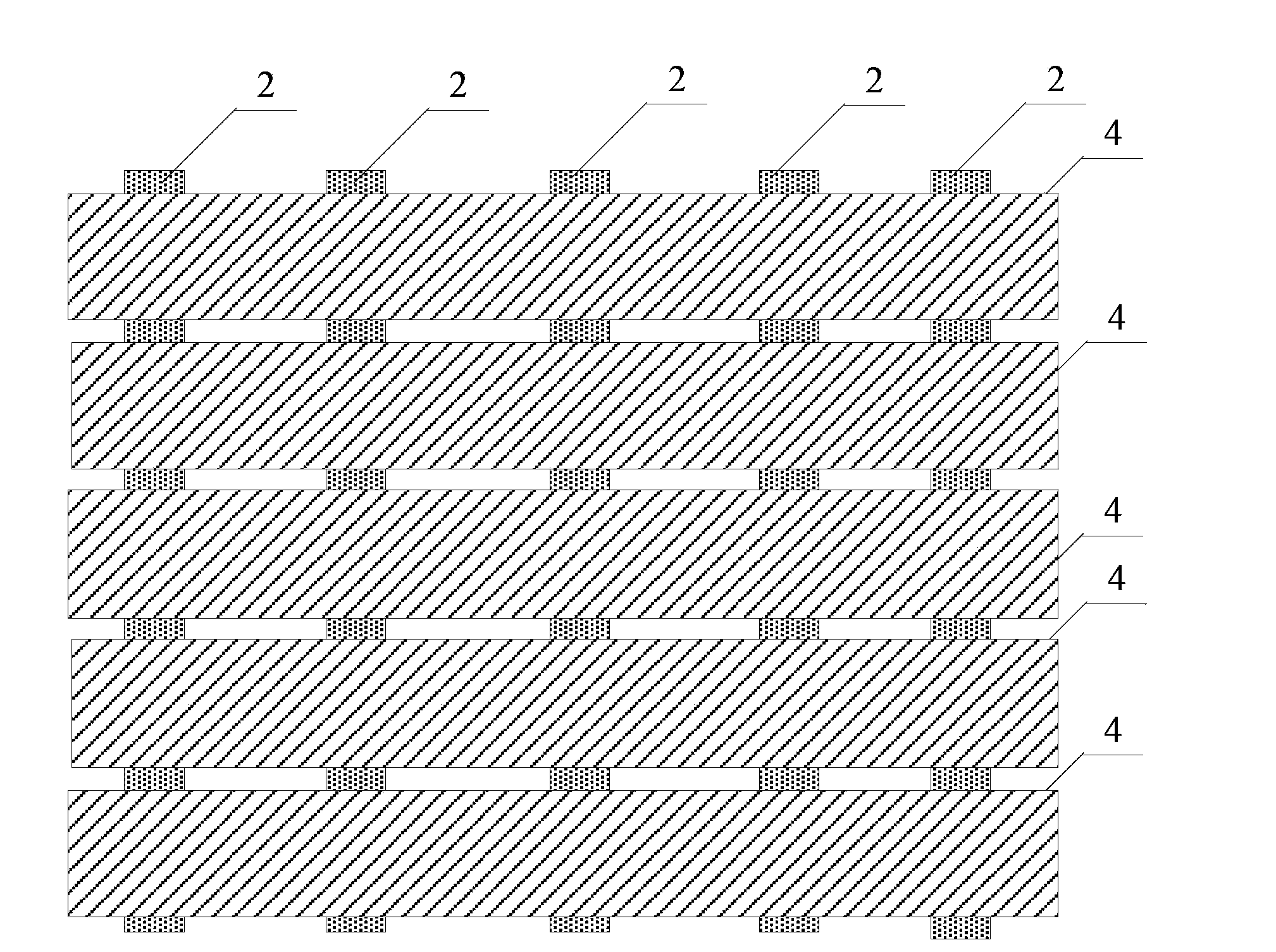
[0024] An embodiment of the present invention provides a touch panel. The touch panel includes a first substrate, and a color filter layer, a plurality of touch sensing electrodes, and a plurality of touch driving electrodes are arranged on the first substrate; a color pixel unit; the touch sensing electrode is arranged between adjacent color pixel units, and has a light-shielding function; the touch driving electrode, which is insulated from the touch sensing electrode and arranged crosswise, is applied with touch scanning during the touch stage signal, the common electrode signal is applied during the display phase.
[0025] Embodiment 1 of the present invention takes the color filter substrate with the color filter layer as the first substrate as an example to describe the touch panel provided by the embodiment of the present invention in detail. The color filter substrate includes a substrate 1, a touch sensing electrode 2, a color filter layer 3 and touch drive electrodes...
Embodiment 2
[0032] Embodiment 2 of the present invention will describe the touch panel in Embodiment 1 in detail in combination with practical applications, but of course it is not limited thereto.
[0033] Such as figure 2 As shown, in order to realize the touch function in the embodiment of the present invention, the touch sensing electrodes 2 and the touch driving electrodes 4 are insulated from each other and intersected. Shading strips 5 can also be provided. If the touch sensing electrodes 2 are arranged between the color pixel units in adjacent columns, the light shielding strips 5 and the touch sensing electrodes 2 are intersected and arranged between the color pixel units in adjacent rows. If the touch sensing electrode 2 is arranged between the color pixel units of adjacent rows, the light-shielding strip 5 and the touch sensing electrode 2 are intersected and arranged between the color pixel units of adjacent columns to better of shading.
[0034] Preferably, the light-shiel...
Embodiment 3
[0040] The embodiment of the present invention is described by taking a transflective display panel as an example, and it is not limited thereto. The color filter substrate in the transflective display panel provided by the embodiment of the present invention has the same structure as that of Embodiment 1 and Embodiment 2, and the embodiment of the present invention will only describe the differences.
[0041] The touch panel provided by the embodiment of the present invention further includes a second substrate opposite to the first substrate. The second substrate in this embodiment may specifically be an array substrate. The schematic diagram of the array substrate is as follows Figure 8 shown. A number of pixel display units arranged in matrix are formed on the second substrate in the same arrangement as the color pixel units arranged in matrix on the first substrate, and a reflective area and a transmissive area are arranged in each pixel display unit to form In the tran...
PUM
 Abstract
Description
Claims
Application Information


