Capacitance fingerprint sensing circuit and sensor

A sensing circuit and sensor technology, applied in the direction of acquiring/organizing fingerprints/palmprints, instruments, characters and pattern recognition, etc., can solve the problems of poor sensitivity of fingerprint sensors, achieve simple structure, improve compatibility, and improve sensitivity Effect

Active Publication Date: 2014-12-17
SHENZHEN GOODIX TECH CO LTD
View PDF3 Cites 45 Cited by
  • Summary
  • Abstract
  • Description
  • Claims
  • Application Information

AI Technical Summary

Problems solved by technology

[0004] The purpose of the embodiments of the present invention is to provide a capacitive fingerprint sensing circuit and sensor, aiming to solve the problem of poor sensitivity of existing fingerprint sensors

Method used


Image

  • Capacitance fingerprint sensing circuit and sensor
  • Capacitance fingerprint sensing circuit and sensor
  • Capacitance fingerprint sensing circuit and sensor

Examples


Embodiment 1

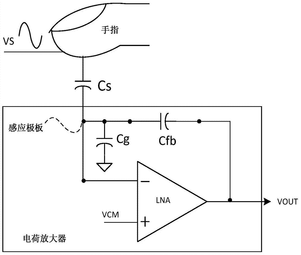
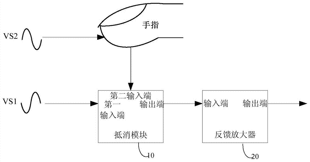
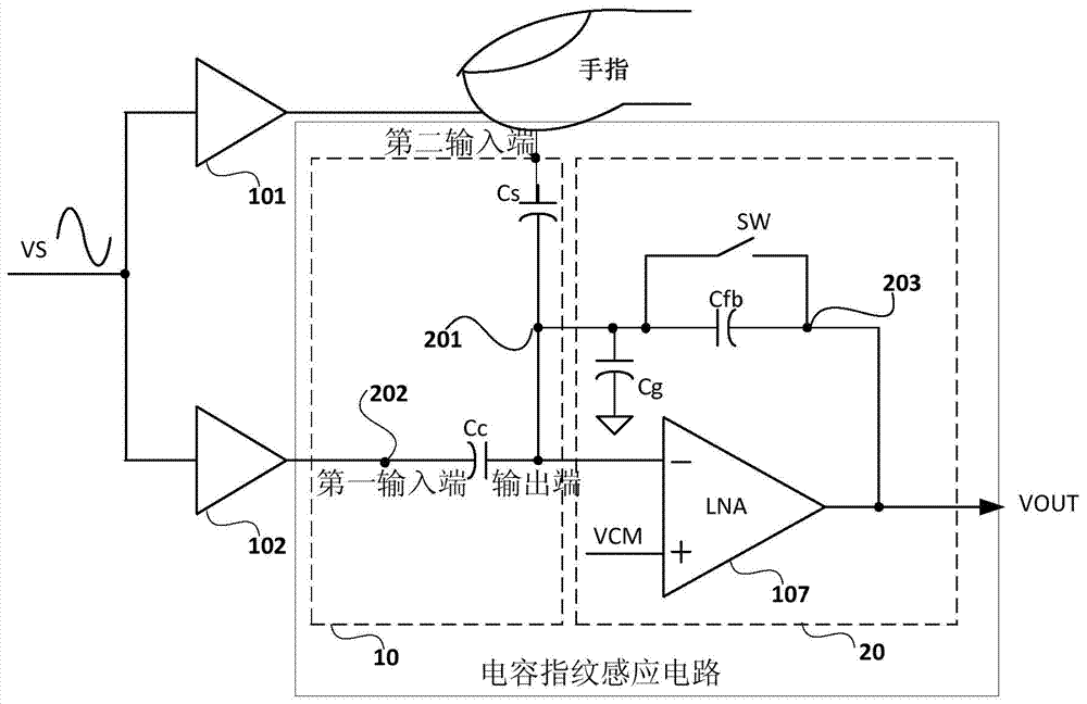
[0024] Embodiment 1 of the present invention proposes a capacitive fingerprint sensing circuit. Such as figure 2 As shown, the capacitive fingerprint sensing circuit of Embodiment 1 of the present invention includes a cancellation module 10 and a feedback amplifier 20, the first input terminal of the cancellation module 10 is connected to the first external drive source VS1, and the second input terminal of the cancellation module 10 is pressed on The finger of the second input terminal is connected to the second external driving source VS2, the output terminal of the canceling module 10 is connected to the input terminal of the feedback amplifier 20, and the signals output by the first external driving source VS1 and the second external driving source VS2 are mutually inverse The signal sent to the cancellation module 10 by the first external driving source VS1 and the signal coupled to the cancellation module 10 by the second external driving source VS2 are cancelled, and t...

Embodiment 2

[0053] In order to achieve sufficient resolution DPI (dots per inch), the available area of ​​the capacitive fingerprint sensing circuit is small, one pixel unit corresponds to one capacitive fingerprint sensing circuit, and the driving amplifier and offset amplifier can be shared by multiple pixel units. Therefore, Embodiment 2 of the present invention proposes a capacitive fingerprint sensor, such as Figure 6 As shown, the capacitive fingerprint sensor according to the second embodiment of the present invention includes a plurality of pixel units, and each pixel unit corresponds to a capacitive fingerprint sensing circuit. It also includes a drive amplifier 401 and a cancellation amplifier 402, the input of the drive amplifier 401 is connected to the external drive source VS, and the output terminal is connected by pressing the finger on the second input terminal of the cancellation module 40 of each capacitive fingerprint sensing circuit to cancel the output of the amplifie...


PUM


Abstract

The invention is applicable to the field of fingerprint identification, and provides a capacitance fingerprint sensing circuit and a sensor. The sensing circuit comprises a counteracting module and a feedback amplifier, wherein the first input end of the counteracting module is connected with a first external driving source; the second input end of the counteracting module is connected with a second external driving source through a finger pressed on the second input end; the output end of the counteracting module is connected with the input end of the feedback amplifier; the phases of signals output by the first external driving source and the second external driving source are opposite to each other; signals accessed into the counteracting module from the first external driving source and signals coupled to the counteracting module from the second external driving source are counteracted so that fingerprint sensing signals relevant to the fingerprint depth are obtained; and the output end of the feedback amplifier outputs amplified fingerprint sensing signals. The capacitance fingerprint sensing circuit and the sensor provided by the embodiment of the invention have the advantages that parts irrelevant to the fingerprint are attenuated through the counteracting module and the external driving sources with opposite phases; only difference mode signals are amplified; and the fingerprint sensing sensitivity is improved.

Description

technical field [0001] The invention belongs to the field of fingerprint identification, in particular to a capacitive fingerprint sensing circuit and a sensor. Background technique [0002] There are differences in the depth of human fingerprints. The convex places are called "ridges" and the concave places are called "valleys". The capacitive fingerprint sensing system utilizes the principle that the sensing capacitance corresponding to the "peak" and "valley" contained in the fingerprint is different, and the amplitude of the output signal is different under the same AC signal excitation, and the image of the "peak" and "valley" The information is converted into corresponding electrical signals. [0003] In order to prevent electrostatic damage to the fingerprint sensor during repeated touches and improve the mechanical strength, it is necessary to place a non-conductive thick dielectric layer (cover) on the surface of the fingerprint sensor to generate dielectric layer-...

Claims


Application Information

Patent Timeline
Patent Type & Authority Applications(China)
IPC IPC(8): G06K9/00
CPCG06V40/1306
Inventor 张均军詹昶
Owner SHENZHEN GOODIX TECH CO LTD
Why Eureka
Try Eureka