Display substrate, manufacturing method of display substrate and liquid crystal display panel

A display substrate and manufacturing method technology, applied in nonlinear optics, instruments, optics, etc., can solve problems such as afterimages in the display area, and achieve the effect of improving display quality

Active Publication Date: 2015-01-21
BOE TECH GRP CO LTD
View PDF4 Cites 10 Cited by
  • Summary
  • Abstract
  • Description
  • Claims
  • Application Information

AI Technical Summary

Problems solved by technology

[0005] The present invention provides a display substrate and its manufacturing method, and a liquid crystal panel, which are used to solve the problem that the charged ions in the non-display area diffuse to the display area, resulting in afterimages around the display area

Method used


Image

  • Display substrate, manufacturing method of display substrate and liquid crystal display panel
  • Display substrate, manufacturing method of display substrate and liquid crystal display panel

Examples


Embodiment 1

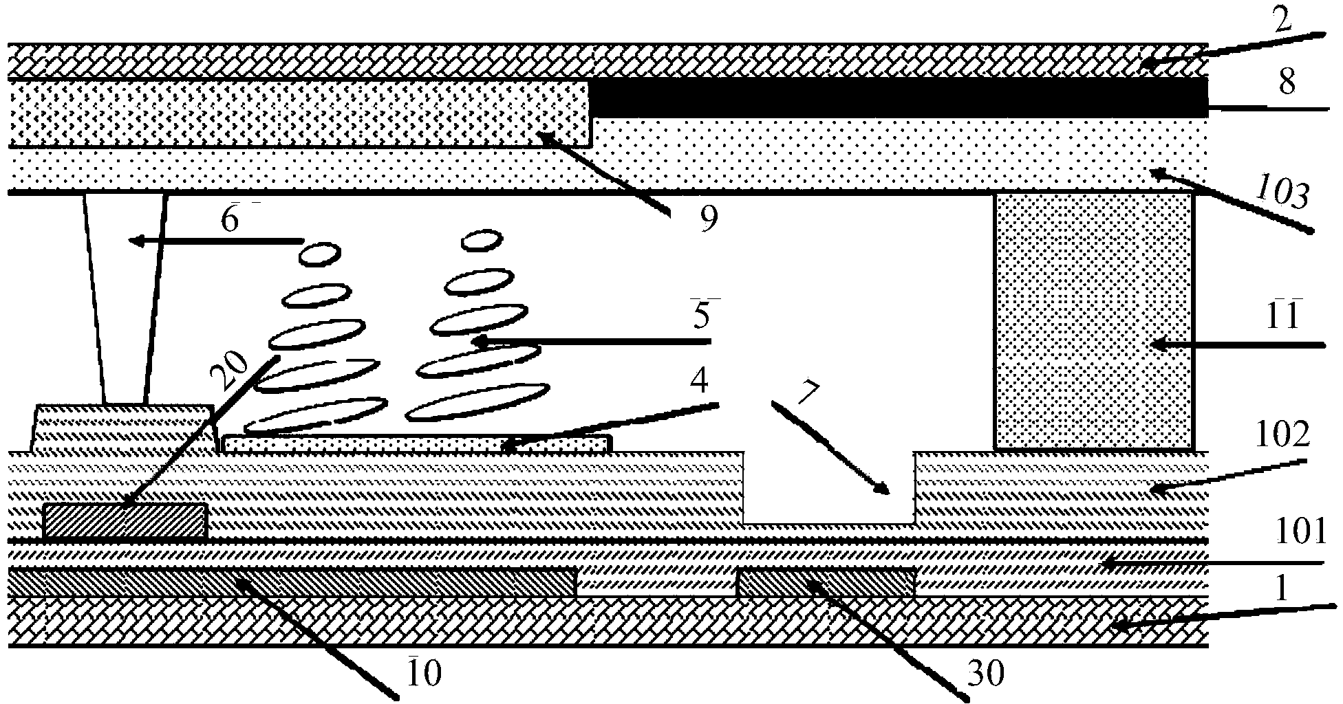
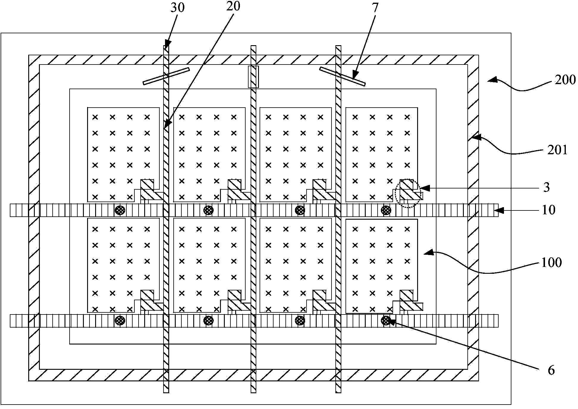
[0020] An embodiment of the present invention provides a display substrate for a liquid crystal panel. The display substrate is specifically an array substrate or a color filter substrate of a liquid crystal panel, including a display area and a non-display area located on the periphery of the display area, and an ion blocking structure is provided in the non-display area of ​​the display substrate to block the non-display area. The charged ions diffuse to the display area.

[0021] The display substrate with the ion blocking structure can significantly improve the afterimage problem around the display area and improve the display quality of the liquid crystal display device.

[0022] In the manufacturing process of liquid crystal panels, charged ions are mainly introduced through two processes of sealant coating and liquid crystal dripping. Based on this, further, the ion blocking structure can be arranged between the sealing area of ​​the non-display area and the display are...

Embodiment 2

[0042] Based on the same inventive concept, an embodiment of the present invention provides a method for manufacturing a display substrate, the display substrate is used for a liquid crystal panel, and includes a display area and a non-display area located on the periphery of the display area.

[0043] Described preparation method comprises:

[0044] An ion blocking structure is formed in the non-display area for blocking charged ions in the non-display area from diffusing to the display area.

[0045] By fabricating the ion blocking structure on the display substrate, the problem of image afterimages around the display area can be significantly improved, and the display quality of the liquid crystal display device can be improved.

[0046] Preferably, the ion blocking structure is located between the sealing area of ​​the display substrate and the display area, and can effectively block charged ions introduced by coating the sealant and liquid crystal dripping from diffusing ...

Embodiment 3

[0090] An embodiment of the present invention also provides a liquid crystal panel, which includes the display substrate in the first embodiment.

[0091] By adopting the liquid crystal panel, the problem of image afterimages around the display area can be effectively solved, and the display quality of the liquid crystal display device can be improved.

[0092] In the technical solution of the present invention, by setting an ion blocking structure in the non-display area of ​​the display substrate, it is used to prevent charged ions in the non-display area from diffusing to the display area, thereby effectively solving the problem of afterimages around the display area and improving the performance of liquid crystal display devices. display quality.


PUM


Abstract

The invention relates to the technical field of liquid crystal displaying and discloses a display substrate, a manufacturing method of the display substrate and a liquid crystal display panel. An ion barrier structure is arranged in a non-display area of the display substrate and used for preventing charged ions in the non-display area from being diffused to a display area, accordingly the problem that residual images are produced on the periphery of the display area can be effectively solved, and the display quality of a liquid crystal display device is improved.

Description

technical field [0001] The invention relates to the technical field of liquid crystal display, in particular to a display substrate, a manufacturing method thereof, and a liquid crystal panel. Background technique [0002] Thin Film Transistor Liquid Crystal Display (TFT-LCD for short) has the characteristics of small size, low power consumption, no radiation, and relatively low manufacturing cost, and occupies a dominant position in the current flat panel display market. The liquid crystal panel is an important part of the liquid crystal display, and it includes an array substrate and a color filter substrate, and the color filter substrate and the array substrate are boxed through a boxing process to form a liquid crystal panel. Among them, the box matching process includes: dripping liquid crystal on one of the array substrate or the color filter substrate through the ODF process, coating the sealant on the other substrate, aligning the array substrate and the color filte...

Claims


Application Information

Patent Timeline
Patent Type & Authority Applications(China)
IPC IPC(8): G02F1/1333
CPCG02F1/1333G02F1/133337
Inventor 赵承潭姚继开铃木照晃周影
Owner BOE TECH GRP CO LTD
Why Eureka
Try Eureka