Pixel structure of CMOS (Complementary Metal-Oxide-Semiconductor Transistor) image sensor and manufacture method thereof

An image sensor and pixel structure technology, which is applied in radiation control devices and other directions, can solve problems such as complex process, leakage current, and low ion implantation energy, and achieve uniform ion distribution, solve afterimage problems, and good control effects

Active Publication Date: 2012-03-21
BRIGATES MICROELECTRONICS KUNSHAN
View PDF1 Cites 0 Cited by
  • Summary
  • Abstract
  • Description
  • Claims
  • Application Information

AI Technical Summary

Problems solved by technology

[0007] The CMOS image sensor in the prior art has at least the following defects: 1. Since the threshold voltage adjustment region 106 uses one-time ion implantation, the depth of the threshold voltage adjustment region 106 formed is difficult to control, which is not suitable for submicron level manufacturing processes; 2. The ion implantation energy of the anti-puncture region 105 is small, generally 40-100KeV, so the depth of the anti-puncture region 105 is not deep enough, resulting in the risk of leakage current under the heavily doped region (also a floating diffusion region) 112; 3. Isolation structure 103 and isolation well 104 are used to isolate photodiodes and transistors from other semiconductor devices, and the process is complex

Method used


Image

  • Pixel structure of CMOS (Complementary Metal-Oxide-Semiconductor Transistor) image sensor and manufacture method thereof
  • Pixel structure of CMOS (Complementary Metal-Oxide-Semiconductor Transistor) image sensor and manufacture method thereof
  • Pixel structure of CMOS (Complementary Metal-Oxide-Semiconductor Transistor) image sensor and manufacture method thereof

Examples


Embodiment Construction

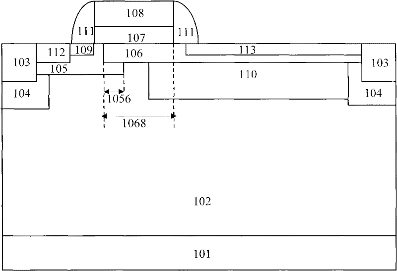
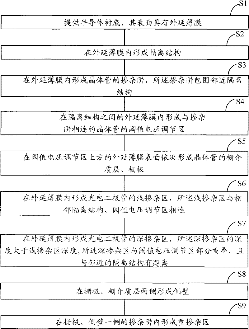
[0046] The inventors have found that the thickness of the threshold voltage adjustment region of the CMOS image sensor in the prior art is difficult to control, and is not suitable for the sub-micron level manufacturing process; There is a risk of leakage current; the isolation structure and isolation well are used to isolate the photodiode and MOS transistor at the same time, and the process is complicated.

[0047] Therefore, the inventor provides a pixel structure of a CMOS image sensor, the structure is as follows:

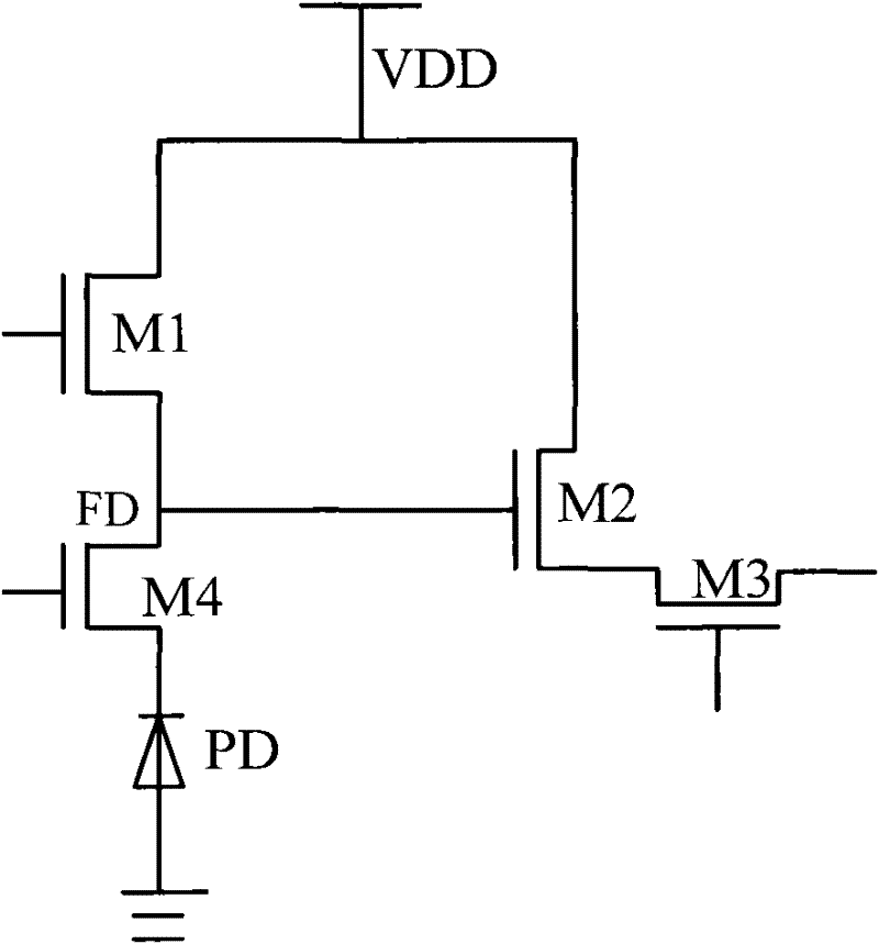
[0048] a semiconductor substrate, an epitaxial film on the substrate, an isolation structure in the epitaxial film, a MOS transistor in the epitaxial film between the isolation structures, and a photodiode adjacent to the MOS transistor, the The MOS transistor includes: a gate dielectric layer and a gate sequentially located on the surface of the epitaxial film, and side walls located on both sides of the gate dielectric layer and the gate;

[0049] a doped w...


PUM


Abstract

The invention relates to a CMOS image sensor comprising a transistor and a photodiode, wherein the transistor comprises a grid dielectric layer and a grid electrode which are arranged on the surface of an epitaxial film in sequence and side walls arranged at both sides of the grid dielectric layer and the grid electrode in sequence, a doping well arranged in the epitaxial film at one side of the grid electrode, heavy-doping regions arranged in doping wells arranged at one side of the grid electrode and one sides of the side walls, and a threshold voltage regulation region arranged in the epitaxial film below the grid electrode, wherein the doping well surrounds an adjacent isolating structure, and the threshold voltage regulation region is adjacent to the doping well. The photodiode comprises a heavy-doping region arranged in the epitaxial film and a light-doping region arranged in the epitaxial film, wherein the heavy-doping region is a distance away from the adjacent isolating structure, the depth of the heavy-doping region is larger than that of the threshold voltage regulation region, and the heavy-doping region and the threshold voltage regulation region are partially overlapped; the conduction type of the light-doping region is opposite to that of the heavy-doping region, the depth of the light-doping region is smaller than that of the heavy-doping region and the light-doping region is adjacent to the isolating structure and the threshold voltage regulation region. The invention reduces the residual image of the image sensor, is suitable for the manufacture process of submicron layer, and has smaller drain current and simple manufacture process.

Description

technical field [0001] The invention relates to a complementary metal oxide semiconductor technology, in particular to a pixel structure of a CMOS image sensor and a manufacturing method thereof. Background technique [0002] Image sensors are divided into complementary metal oxide (CMOS) image sensors and charge-coupled device (CCD) image sensors, which are generally used to convert optical signals into corresponding electrical signals. The advantage of the CCD image sensor is that it has high image sensitivity and low noise, but it is difficult to integrate the CCD image sensor with other devices, and the power consumption of the CCD image sensor is relatively high. In contrast, CMOS image sensors have the advantages of simple process, easy integration with other devices, small size, light weight, low power consumption, and low cost. At present, CMOS image sensors have been widely used in still digital cameras, camera phones, digital video cameras, medical imaging devices...

Claims


Application Information

Patent Timeline
Patent Type & Authority Patents(China)
IPC IPC(8): H01L27/146
Inventor 余泳
Owner BRIGATES MICROELECTRONICS KUNSHAN
Why Eureka
Try Eureka