Doped-absorber graded transition enhanced multiplication avalanche photodetector

a photodetector and graded transition technology, applied in the field of optoelectronic communication systems, can solve the problems of reducing the maximum achievable gain, reducing the thickness of the absorption layer, and reducing the quantum efficiency, so as to achieve the effect of reducing the barrier to electron transpor

Active Publication Date: 2007-01-09
QORVO US INC
View PDF6 Cites 23 Cited by
  • Summary
  • Abstract
  • Description
  • Claims
  • Application Information

AI Technical Summary

Benefits of technology

[0009]According to one exemplary embodiment, the present invention provides an avalanche photodetector including an absorption layer, a multiplication region including at least one multiplication layer, and a graded transition region between the absorption layer and the multiplication region. The graded transition region is a graded-bandgap region including a graded conduction band energy level that produces a gradual change between the conduction band energy level of the absorber layer and a conduction band energy level of the multiplication region. Together with an applied operating bias, the graded transition region alleviates the barrier to electron transport that exists due to the potential energy difference between the absorption layer and the multiplication region.

Problems solved by technology

An undesired consequence of the reduction of absorption layer thickness is lower quantum efficiency.
Decreasing the width of the multiplication region to improve bandwidth performance, however, also lowers the maximum achievable gain.
Although a superlattice structure achieves more avalanche gain per unit length than a homogeneous material, it is unlikely that such superlattice structures are optimal in this regard, especially in relatively short multiplication regions.
Additionally, the use of a superlattice structure may produce dark current effects that can adversely affect the signal.

Method used


Image

  • Doped-absorber graded transition enhanced multiplication avalanche photodetector
  • Doped-absorber graded transition enhanced multiplication avalanche photodetector
  • Doped-absorber graded transition enhanced multiplication avalanche photodetector

Examples


Embodiment Construction

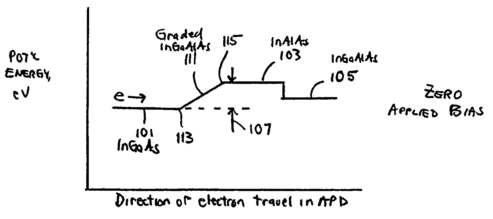
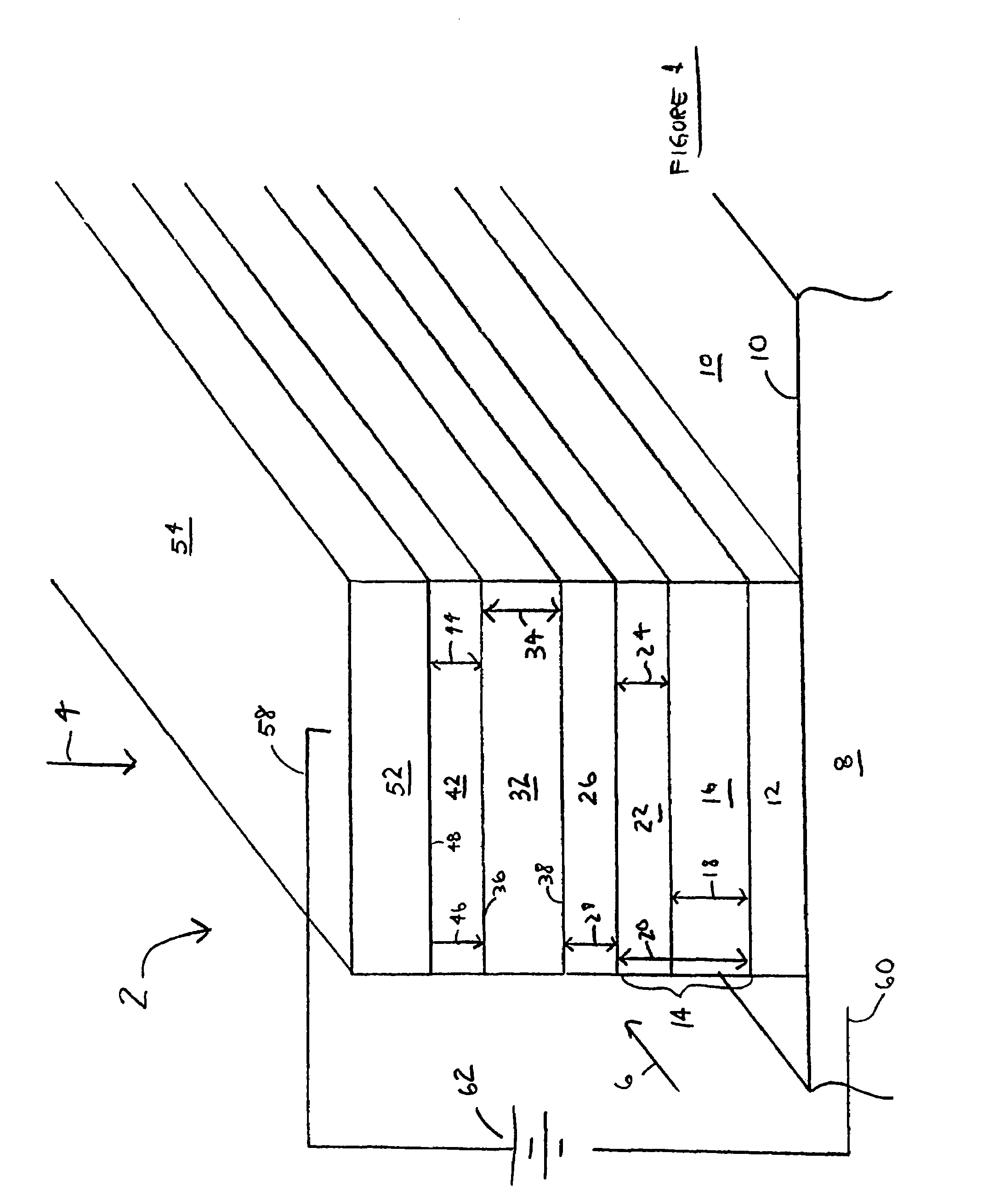
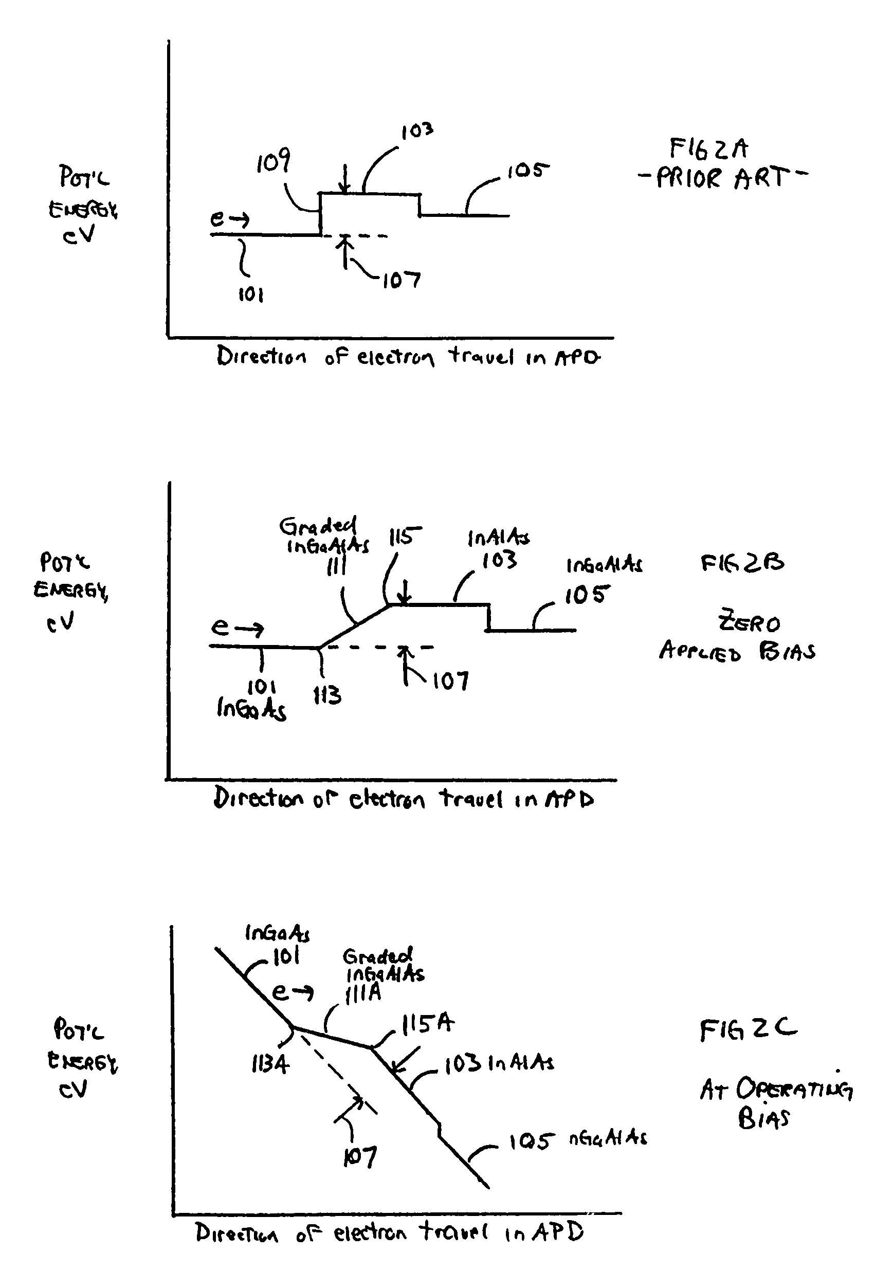
[0017]In one exemplary embodiment, the present invention provides an APD including a graded transition region formed between an absorption layer and the multiplication region of the APD. This graded-bandgap, graded transition region, in conjunction with an applied operating bias, helps to overcome the potential energy barrier an electron must overcome in traversing from the absorption layer to the multiplication region. In another exemplary embodiment, the present invention provides a P-type dopant impurity introduced into the absorption region of an APD to move the P-side depletion region edge closer to the multiplication region. The P-type dopant impurity concentration includes a gradient that decreases within the absorption layer along the direction towards the multiplication region. According to another exemplary embodiment, the present invention provides a relatively wide, two layer multiplication region to increase gain in the multiplication region. The present invention there...


PUM


Abstract

An InGaAs/InAlAs-based avalanche photodetector provides high gain and high bandwidth over a range of operating biases. A graded transition region alleviates the barrier to electron transport from the absorption region to the multiplication region when an operating bias is applied. The graded transition region is a graded bandgap material with a relatively wide bandwidth in the region closer to the multiplication region and a relatively narrow bandgap in the region closer to the absorption region. In another embodiment, a p-type dopant profile is introduced within the absorption layer to produce an electrostatic field which accelerates electrons towards the multiplication region. In another embodiment, a bi-level multiplication region with a wide bandgap ternary layer and a narrower bandgap quarternary layer is provided at an increased thickness to improve gain per unit length.

Description

CROSS-REFERENCE TO RELATED APPLICATION[0001]This application claims the benefit U.S. Provisional Application No. 60 / 432,926, filed Dec. 12, 2002, the contents of which are incorporated fully herein.FIELD OF THE INVENTION[0002]The present invention relates generally to optoelectronic communication systems. More particularly, the present invention relates to an avalanche photodetector and the process for forming the same.BACKGROUND OF THE INVENTION[0003]Avalanche photodetectors (APDs) are used in a wide variety of applications in today's advancing optoelectronics industry. For example, avalanche photodetectors are commonly used as optical monitors and optical receivers.[0004]When light, i.e., an optical signal, is directed to and absorbed by an absorption layer of an APD, electron-hole pairs are created and an electrical current is generated thereby converting the optical signal to an electrical signal. It is desirable to produce APDs with high quantum efficiency, high gain and high b...

Claims


Application Information

Patent Timeline
Patent Type & Authority Patents(United States)
IPC IPC(8): H01L27/15
CPCH01L31/035236B82Y20/00H01L31/1075H01L31/02327
Inventor YODER, PAUL DOUGLAS
Owner QORVO US INC
Why Eureka
Try Eureka