Low leakage heterojunction vertical transistors and high performance devices thereof

A technology of field effect transistors and vertical channels, which is applied in the direction of transistors, semiconductor devices, semiconductor/solid-state device manufacturing, etc., and can solve problems such as short channel effects

Inactive Publication Date: 2005-02-02
IBM CORP
View PDF3 Cites 23 Cited by
  • Summary
  • Abstract
  • Description
  • Claims
  • Application Information

AI Technical Summary

Problems solved by technology

However, two outstanding issues remain in these planar devices: device scaling and control of short-channel effects.
However, it is a planar structure and still has the problem of short trench effect

Method used


Image

  • Low leakage heterojunction vertical transistors and high performance devices thereof
  • Low leakage heterojunction vertical transistors and high performance devices thereof
  • Low leakage heterojunction vertical transistors and high performance devices thereof

Examples


Embodiment Construction

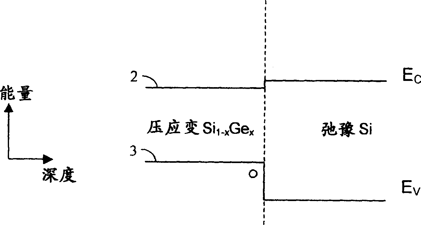
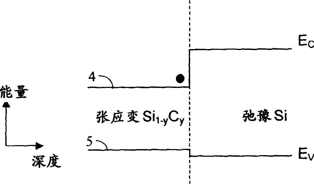
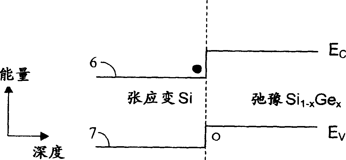
[0029] The lattice constants of carbon, silicon, and germanium are 3.567 angstroms, 5.431 angstroms, and 5.646 angstroms, respectively. In pseudomorphic SiC on relaxed Si, or pseudomorphic Si on relaxed SiGe or Ge substrates, there is biaxial tensile strain, which means that in pseudomorphic materials, in the growth plane (surface) the lattice The constant is larger and the lattice constant is smaller along the growth direction (perpendicular to the surface). On the other hand, in pseudomorphic SiGe on relaxed Si, or pseudocrystalline Ge on relaxed SiGe, there is compressive strain, which means that in pseudomorphic materials, the lattice constant is much lower in the growth plane (surface). Small and larger along the growth direction (perpendicular to the surface) lattice constant. The addition of small amounts of carbon (figure 1 The conduction and valence bands of compressively strained SiGe or SiGe(C) on relaxed silicon are shown by curves 2 and 3, respectively. The hole...


PUM


Abstract

A method for forming and the structure of a vertical channel of a field effect transistor, a field effect transistor and CMOS circuitry are described incorporating a drain, body and source region on a sidewall of a vertical single crystal semiconductor structure wherein a hetero-junction is formed between the source and body of the transistor, wherein the source region and channel are independently lattice strained with respect the body region and wherein the drain region contains a carbon doped region to prevent the diffusion of dopants (i.e., B and P) into the body. The invention reduces the problem of short channel effects such as drain induced barrier lowering and the leakage current from the source to drain regions via the hetero-junction and while independently permitting lattice strain in the channel region for increased mobility via choice of the semiconductor materials. The problem of scalability of the gate length below 100 nm is overcome by the heterojunction between the source and body regions.

Description

[0001] Cross References to Related Applications [0002] This application is further cross-referenced to the following application: U.S. Patent Application No. 10 / 463038 (Attorney Docket No. YOR920030140US1), inventors Q. Quyang and Jack O. Chu, entitled "Ultra-Scalable High-Speed ​​Heterojunction Vertical N-Channel MISFETs and Methods Thereof (Ultra Scalable High Speed ​​Heterojunction Vertical N-channel MISFETs and Methods Thereof), which relates to Vertical N-channel MISFETs, is hereby incorporated by reference and hereby assigned to the assignee. [0003] This application further cross-references the following application: U.S. Patent Application No. 10 / 462933 (Attorney Docket No. YOR920030141US1), inventors Q. Quyang and Jack O. Chu, entitled "High-Speed ​​Lateral "High Speed ​​Lateral Heterojunction MISFETs Realized by 2-dimensional Bandgap Engineering and Method Thereof," which relates to Lateral Heterojunction MISFETs, is hereby incorporated by reference and hereby assig...

Claims


Application Information

Patent Timeline
Patent Type & Authority Applications(China)
IPC IPC(8): H01L27/092H01L21/336H01L21/8238H01L29/12H01L29/78H01L29/786
CPCH01L21/823807H01L29/165H01L29/045H01L29/778H01L21/823885H01L29/161H01L29/7781H01L29/7828H01L29/7789H01L29/7782
Inventor 欧阳齐庆赵泽安
Owner IBM CORP
Why Eureka
Try Eureka