Negative capacitance semiconductor sensor

a negative capacitance, semiconductor sensor technology, applied in the field of semiconductor sensors, can solve the problems of insufficient detection theoretical upper limit of sensitivity of conventional sensors, etc., and achieve the effect of increasing the performance of conventional semiconductor sensors and in particular their sensitivity

Active Publication Date: 2022-03-29
ECOLE POLYTECHNIQUE FEDERALE DE LAUSANNE (EPFL)
View PDF7 Cites 0 Cited by
  • Summary
  • Abstract
  • Description
  • Claims
  • Application Information

AI Technical Summary

Benefits of technology

[0006]It is an object of the present invention to increase the performance of conventional semiconductor sensors and in particular their sensitivity.
[0008]The proposed new solution has the advantage that the sensitivity of the semiconductor sensor can be increased compared with conventional semiconductor sensors, which do not exploit the benefits of negative capacitance. Furthermore, the proposed solution is very energy efficient (higher current efficiency with respect to standard semiconductor sensors) and can thus be used in low power applications.

Problems solved by technology

Conventional ISFETs have a theoretical upper limit for their sensitivity.
However, in some cases, even a proportionally small variation in the biomarker concentration can be relevant, but the sensitivity of conventional sensors may be insufficient to detect it, especially if the measurement conditions are not ideal and noise is added to the system, which is often the case when using e.g. wearable devices or point of care devices.

Method used


Image

  • Negative capacitance semiconductor sensor
  • Negative capacitance semiconductor sensor
  • Negative capacitance semiconductor sensor

Examples


first embodiment

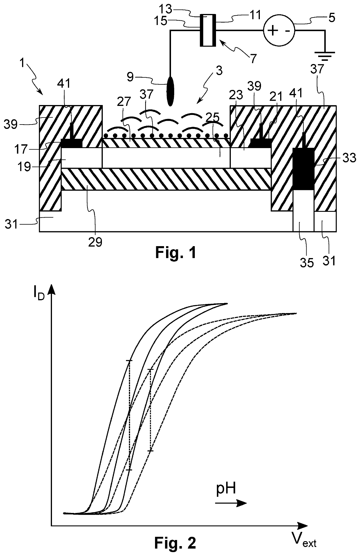
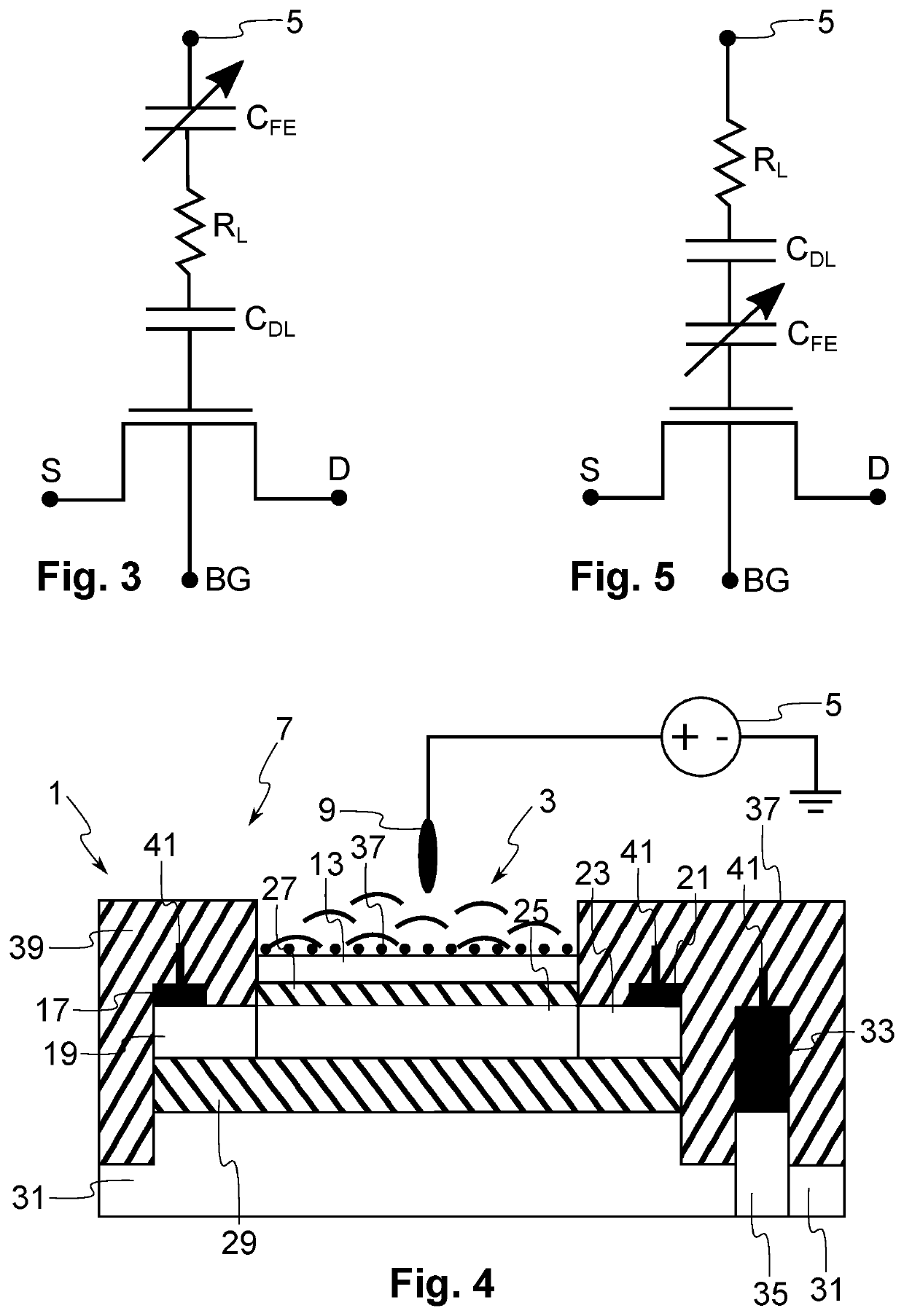
[0023]FIG. 1 is a schematic view of a multi-gate chemical sensor 1, also referred to as a device, comprising two physically independent or separate gates according to the present invention. In the present description, by a multi-gate device is understood a device comprising at least two gate elements, nodes, terminals or regions. Thus, the device of FIG. 1 could comprise more than two gates. However, the teachings of the present invention are equally applicable to chemical sensors having only one gate element. The sensor 1 of FIG. 1 comprises a field-effect transistor (FET) exposed to a liquid solution 3. As can be seen in FIG. 1, the sensor comprises an external input bias source or node 5, which in this example is a voltage source. The external input bias source is configured to generate a periodic external sensor electrical bias function or signal. It is to be noted that the word “signal” is used in the present description in its broad sense and does not imply that any informatio...

fourth embodiment

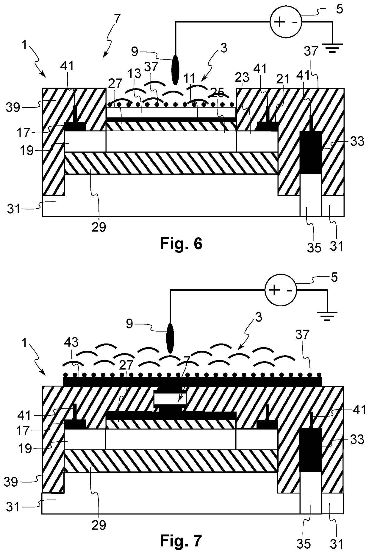
[0036]FIG. 7 illustrates the present invention. According to this embodiment, the transistor has an extended gate configuration, where the Fe—C 7 is interposed between the gate oxide (i.e. the first insulator 27) of the transistor and the area or surface exposed to the solution 3. The Fe—C can be positioned on top of the gate oxide, at the other end of the extended gate or in any position between these two extremes. In this example and as is shown in FIG. 7, the front gate comprises an electrically conductive element 43 deposited on top of the first insulator 27, which then extends upwards to form an extended gate configuration. This electrically conductive element is interrupted by the Fe—C 7 as is shown in FIG. 7. Thus, according to this embodiment, there is a through hole in the third insulator 39 for the front gate contact 43 to pass through it to reach the top surface of the first dielectric layer 27. The front gate metal contact forms a substantially flat longitudinal contact ...


PUM

PropertyMeasurementUnit
thicknessaaaaaaaaaa
gate bias voltageaaaaaaaaaa
thicknessaaaaaaaaaa

Abstract

A semiconductor sensor includes a source element; a drain element; and a semiconductor channel element between the source element and the drain element, forming an electrically conductive channel. An insulator is positioned between the semiconductor channel element and a solution to be sensed. A reference contacts the solution and sets an electric potential of the solution. A bias voltage source generates an external sensor bias voltage for electrically biasing the reference electrode. A sensing surface interacts with the solution comprising analytes for generating a surface potential change at the sensing surface dependent on the concentration of analytes. The sensor further includes a ferroelectric capacitance element between the insulator and the bias voltage source for generating a negative capacitance for a differential gain between the external sensor bias voltage and an internal sensor bias voltage sensed at a surface of the channel element facing the insulator or ferroelectric capacitance element.

Description

TECHNICAL FIELD[0001]The present invention relates to a semiconductor sensor, such as an ion-sensitive field-effect transistor (ISFET), chemical field-effect transistor (Chem FET), field-effect transistor-based biosensor (BioFET), or their respective counterparts based on other kinds of semiconductor sensors, such as tunnel field-effect transistors (TFETs). More specifically, the proposed sensor exploits the negative capacitance effect of a ferroelectric material to improve its performance.BACKGROUND OF THE INVENTION[0002]The first type of field-effect transistor chemical sensor was first introduced by Bergveld in the early 70s. It provided a semiconductor alternative to the glass electrodes for pH and ion measurements. In its simplest form, a FET chemical sensor or an ISFET is comparable to a planar metal-oxide-semiconductor field-effect transistor (MOSFET) except that the gate electrode directly in contact with the gate dielectric is instead replaced by a reference electrode actin...

Claims


Application Information

Patent Timeline
Patent Type & Authority Patents(United States)
IPC IPC(8): H01L29/78G01N27/414H01L29/66H01L29/51
CPCH01L29/78391G01N27/4145H01L29/513H01L29/6684H01L29/66568
Inventor IONESCU, MIHAI ADRIANBELLANDO, FRANCESCOSAEIDI, ALI
Owner ECOLE POLYTECHNIQUE FEDERALE DE LAUSANNE (EPFL)
Why Eureka
Try Eureka