Vertical interconnect elevator based on through silicon vias

a vertical interconnect elevator and silicon via technology, applied in the direction of semiconductor devices, electrical equipment, semiconductor/solid-state device details, etc., can solve the problems of higher fabrication cost, lower fabrication yield, and more power consumption, so as to accelerate workload processing or application, reduce nre cost, and reduce non-recurring engineering costs

Pending Publication Date: 2021-02-11
ICOMETRUE CO LTD
View PDF4 Cites 24 Cited by
  • Summary
  • Abstract
  • Description
  • Claims
  • Application Information

AI Technical Summary

Benefits of technology

[0036]The IAC IC chip is designed, implemented and fabricated using varieties of semiconductor technology nodes or generations, including old or matured technology nodes or generations, for example, less advanced than or equal to, or more mature than 20 nm or 30 nm, and for example using the technology node of 22 nm, 28 nm, 40 nm, 90 nm, 130 nm, 180 nm, 250 nm, 350 nm or 500 nm. The semiconductor technology node or generation used in the IAC IC chip is 1, 2, 3, 4, 5 or greater than 5 nodes or generations older, more matured or less advanced than that used in the standard commodity FPGA IC chip packaged in the same logic drive. Transistors used in the IAC IC chip may be a FINFET, a Fully Depleted Silicon-on-insulator (FDSOI) MOSFET, a Partially Depleted Silicon-On-Insulator (PDSOI) MOSFET or a conventional planar MOSFET. Transistors used in the IAC IC chip may be different from that used in the standard commodity FPGA IC chip packaged in the same logic drive; for example, the IAC IC chip may use the conventional planar MOSFET, while the standard commodity FPGA IC chip packaged in the same logic drive may use the FINFET or GAAFET; or the IAC IC chip may use the Fully Depleted Silicon-on-insulator (FDSOI) MOSFET, while the standard commodity FPGA IC chips packaged in the same logic drive may use the FINFET. Since the IAC IC chip in this aspect of disclosure may be designed and fabricated using older or less advanced technology nodes or generations, its NRE cost is cheaper than or less than that of the current ASIC or COT IC chip designed and fabricated using an advanced IC technology node or generation. The NRE cost for designing a current ASIC or COT IC chip using an advanced IC technology node or generation, for example, more advanced than or below 20 nm or 10 nm, may be more than US $5M, US $10M, US $20M or even exceeding US $50M, or US $100M. The cost of a photo mask set for an ASIC or COT IC chip at the 16 nm technology node or generation is over US $2M, US $5M, or US $10M. Implementing the same or similar innovation and / or application using the logic drive including the IAC IC chip designed and fabricated using more matured or less advanced technology nodes or generations may reduce NRE cost down to less than US $10M, US $7M, US $5M, US $3M or US $1M. Compared to the implementation by developing the current logic ASIC or COT IC chip, the NRE cost of developing the IAC IC chip for use in the standard commodity logic drive to achieve the same or similar innovation and / or application may be reduced by a factor of 2, 5, 10, 20, or 30.
[0042]Another aspect of the disclosure provides a method to reduce Non-Recurring Engineering (NRE) expenses for implementing (i) an innovation, (ii) an innovation process or application, and / or (iii) accelerating workload processing or application in semiconductor IC chips by using the standardized commodity logic drive, FIG. 36. The standardized commodity logic drive may comprise one or a plurality of FPGA IC chips, one or a plurality of HBM IC chips or one or a plurality of HBM SCSPs, one or a plurality of non-volatile memory IC chips, and / or one or a plurality of auxiliary or supporting IC chips. The standardized commodity logic drive may be packaged in a multichip package, such as the FPGA / HBM CSP, the FPGA / AS CSP or the 3D stacked chip package, as described and specified above. A person, user, or developer with an innovation and / or an application concept or idea or an aim for accelerating workload processing may purchase the standardized commodity logic drive and develop or write software codes or programs to load into the standardized commodity logic drive to implement his / her innovation and / or application concept or idea; wherein said innovation and / or application (maybe abbreviated as innovation below) comprises (i) innovative algorithms and / or architectures of computing, processing, learning and / or inferencing, and / or (ii) innovative and / or specific applications. The developed software codes or programs related to the innovation are used for configuring the one or a plurality of FPGA IC chips in the multichip package, and may be stored in the one or a plurality of non-volatile memory IC chips in the same multichip package. With non-volatile memory cells in the one or a plurality of non-volatile memory IC chips in the multichip package, the logic drive may be used as an alternative of the ASIC chip fabricated using advanced technology nodes. The standard commodity logic drive comprises one or a plurality of FPGA IC chips fabricated by using advanced technology nodes or generations more advanced than 20 nm or 10 nm. The innovation is implemented in the logic drive by configuring the hardware of FPGA IC chips by altering the data in the 5T or 6T SRAM cells of the programmable interconnection (configurable switches including pass / no-pass switching gates and multiplexers) and / or programmable logic circuits, cells or blocks (including LUTs and multiplexers) therein using the data stored in the non-volatile memory cells in the one or a plurality of non-volatile memory IC chips or the one or a plurality of FPGA IC chips in the multichip package. Compared to the implementation by developing a logic ASIC or COT IC chip, implementing the same or similar innovation and / or application using the logic drive may reduce the NRE cost down to smaller than US $1M by developing a software and installing it in the purchased or rented standard commodity logic drive. The aspect of the disclosure inspires the innovation and lowers the barrier for implementing the innovation in IC chips designed and fabricated using an advanced IC technology node or generation, for example, a technology node or generation more advanced than or below 20 nm or 10 nm.
[0043]Another aspect of the disclosure provides a “public innovation platform” by using logic drives for innovators to easily and cheaply implement or realize their innovation (algorithms, architectures and / or applications) in semiconductor IC chips fabricated using advanced IC technology nodes more advanced than 20 nm or 10 nm, and for example, using a technology node of 16 nm, 10 nm, 7 nm, 5 nm or 3 nm, FIG. 36. In early days, 1990's, innovators could implement their innovation (algorithms, architectures and / or applications) by designing IC chips and fabricate their designed IC chips in a semiconductor foundry fab using technology nodes at 1 μm, 0.8 μm, 0.5 μm, 0.35 μm, 0.18 μm or 0.13 μm, at a cost of about several hundred thousands of US dollars. The IC foundry fab was then the “public innovation platform”. However, when IC technology nodes migrate to a technology node more advanced than 20 nm or 10 nm, and for example to the technology node of 16 nm, 10 nm, 7 nm, 5 nm or 3 nm, only a few giant system or IC design companies, not the public innovators, can afford to use the semiconductor IC foundry fab. It costs about or over 5 million US dollars to develop and implement an IC chip using these advanced technology nodes. The semiconductor IC foundry fab is now not “public innovation platform” anymore, it is “club innovation platform” for club innovators only. The concept of the disclosed logic drives, comprising standard commodity FPGA IC chips, provides public innovators “public innovation platform” back to semiconductor IC industry again; just as in 1990's. The innovators can implement or realize their innovation (algorithms, architectures and / or applications) by using logic drives (comprising FPGA IC chips fabricated using advanced than 20 nm or 10 nm technology nodes) and writing software programs in common programming languages, for example, C, Java, C++, C#, Scala, Swift, Matlab, Assembly Language, Pascal, Python, Visual Basic, PL / SQL or JavaScript languages, at a cost of less than 500K or 300K US dollars. The innovators can install their developed software using their own standard commodity logic drives or rented standard commodity logic drives in data centers or clouds through networks.
[0044]Another aspect of the disclosure provides a method to change the current logic ASIC or COT IC chip business into a commodity logic IC chip business, like the current commodity DRAM, or commodity NAND flash memory IC chip business, by using the standardized commodity logic drive. Since the performance, power consumption, and engineering and manufacturing costs of the standardized commodity logic drive may be better than that of the ASIC or COT IC chip for a same innovation (algorithms, architectures and / or applications) or an aim for accelerating workload processing, the standardized commodity logic drive may be used as an alternative for designing an ASIC or COT IC chip. The current logic ASIC or COT IC chip design, manufacturing and / or product companies (including fabless IC design and product companies, IC foundry or contracted manufactures (may be product-less), and / or vertically-integrated IC design, manufacturing and product companies) may become companies like the current commodity DRAM, or NAND flash memory IC chip design, manufacturing, and / or product companies; or like the current DRAM module design, manufacturing, and / or product companies; or like the current flash memory module, flash USB stick or drive, or flash solid-state drive or disk drive design, manufacturing, and / or product companies.

Problems solved by technology

The switch from the FPGA design to the ASIC or COT design is because the current FPGA IC chip, for a given application and compared with an ASIC or COT chip, (1) has a larger semiconductor chip size, lower fabrication yield, and higher fabrication cost, (2) consumes more power, and (3) gives lower performance.
The high NRE cost in implementing the innovation and / or application using the advanced IC technology nodes or generations slows down or even stops the innovation and / or application using advanced and powerful semiconductor technology nodes or generations.

Method used


Image

  • Vertical interconnect elevator based on through silicon vias
  • Vertical interconnect elevator based on through silicon vias
  • Vertical interconnect elevator based on through silicon vias

Examples


Embodiment Construction

for a more effective presentation. Conversely, some embodiments may be practiced without all of the details that are disclosed.

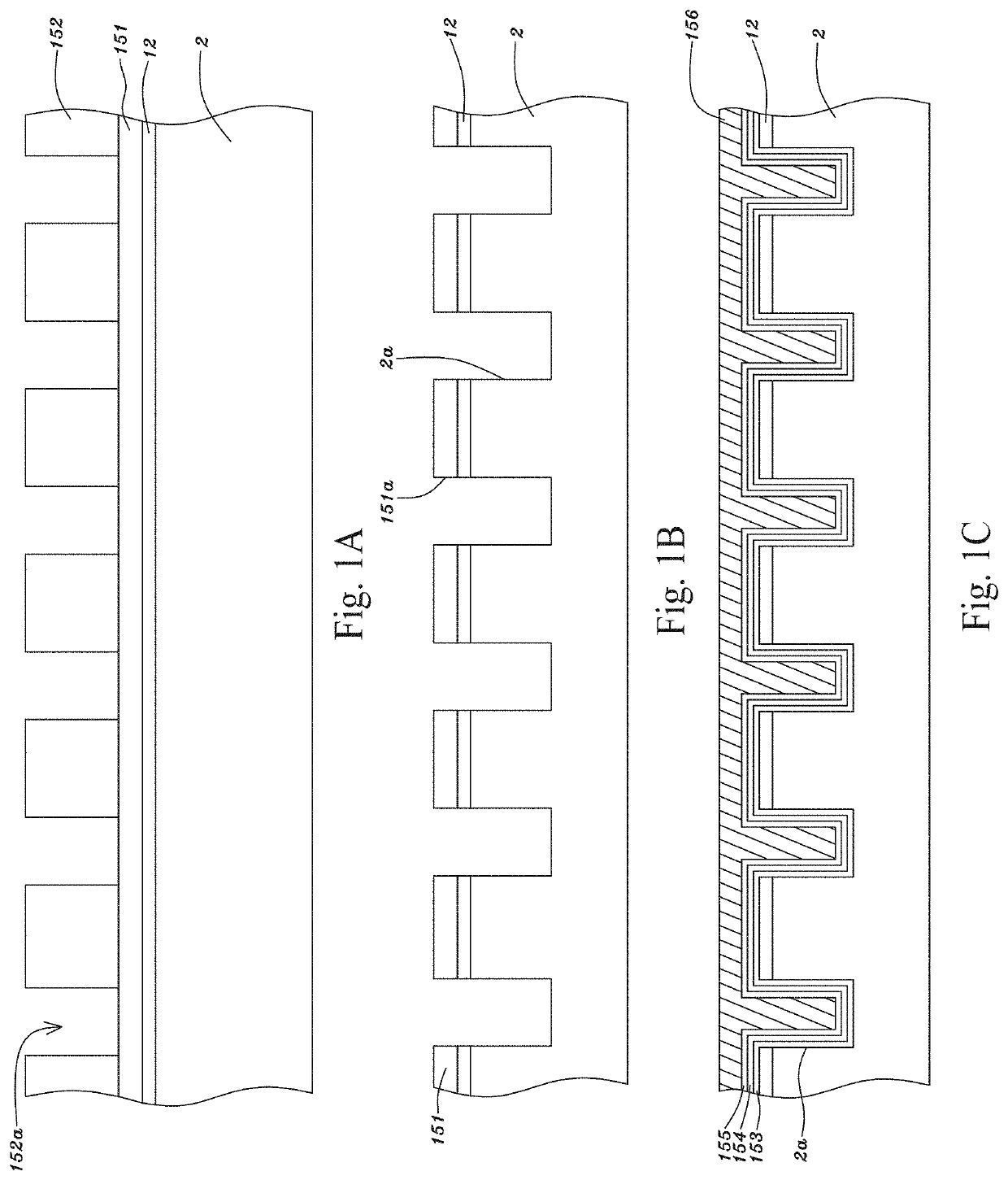
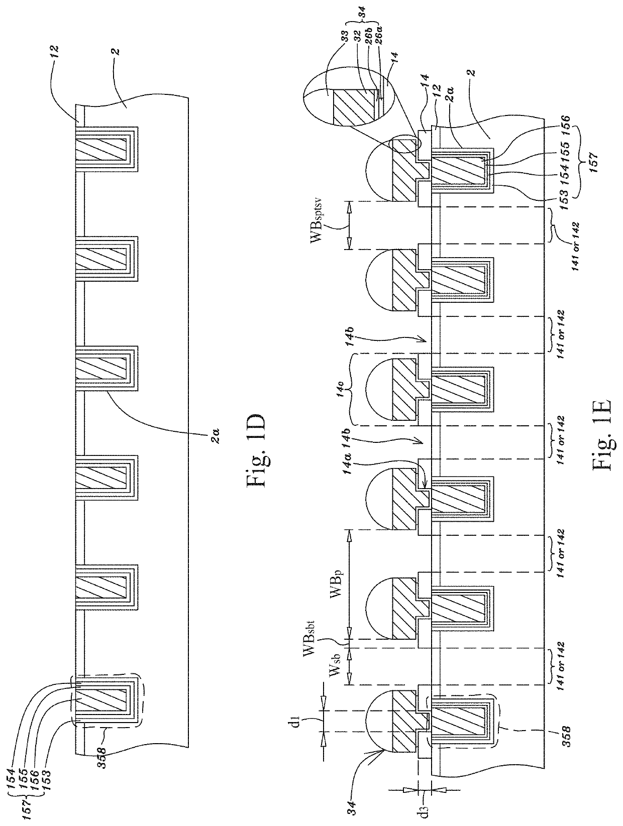
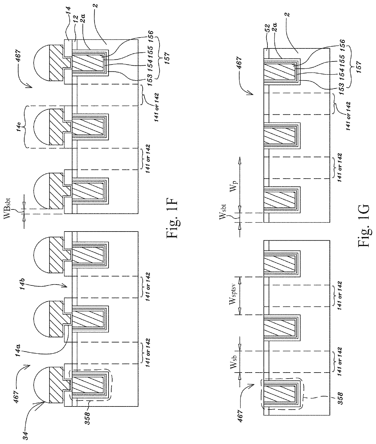
[0112]Specification and Process for First and Second Types of Vertical-Through-Via (VTV) Connectors (Vertical-Interconnect-Elevator (VIE) Chips or Components) Processed from Through-Silicon-Via (TSV) Wafer(s)

[0113]A vertical-through-via (VTV) connector is provided with multiple vertical through vias (VTVs) for vertical connection to transmit signals or clocks or deliver power or ground in a vertical direction. The vertical-through-via (VTV) connector may be processed from one or more through-silicon-via (TSV) wafer(s), mentioned as below:

[0114]1. First and Second Types of Vertical-Through-Via (VTV) Connectors for Through-Silicon-Via Interconnect Elevators (TSVIEs) Processed from Single-Layered Through-Silicon-Via (TSV) Wafers

[0115]FIGS. 1A-1G are schematically cross-sectional views showing a process for forming first and second types of vertical-through-via ...


PUM

PropertyMeasurementUnit
insulatingaaaaaaaaaa
widthaaaaaaaaaa
thermoelectricaaaaaaaaaa

Abstract

A chip package includes a first integrated-circuit (IC) chip; a second integrated-circuit (IC) chip over the first integrated-circuit (IC) chip; a connector over the first integrated-circuit (IC) chip and on a same horizontal level as the second integrated-circuit (IC) chip, wherein the connector comprises a substrate over the first integrated-circuit (IC) chip and a plurality of through vias vertically extending through the substrate of the connector; a polymer layer over the first integrated-circuit (IC) chip, wherein the polymer layer has a portion between the second integrated-circuit (IC) chip and connector, wherein the polymer layer has a top surface coplanar with a top surface of the second integrated-circuit (IC) chip, a top surface of the substrate of the connector and a top surface of each of the plurality of through vias; and an interconnection scheme on the top surface of the polymer layer, the top surface of the second integrated-circuit (IC) chip, the top surface of the connector and the top surface of each of the plurality of through vias.

Description

PRIORITY CLAIM[0001]This application claims priority benefits from U.S. provisional application No. 62 / 882,941, filed on Aug. 5, 2019 and entitled “VERTICAL INTERCONNECT ELEVATOR BASED ON THROUGH SILICON VIAS”, U.S. provisional application No. 62 / 891,386, filed on Aug. 25, 2019 and entitled “VERTICAL INTERCONNECT ELEVATOR BASED ON THROUGH SILICON VIAS”, U.S. provisional application No. 62 / 903,655, filed on Sep. 20, 2019 and entitled “3D CHIP PACKAGE BASED ON THROUGH-SILICON-VIA INTERCONNECTION ELEVATOR”, U.S. provisional application No. 62 / 964,627, filed on Jan. 22, 2020 and entitled “3D chiplet system-in-a-package using vertical-through-via connector”, U.S. provisional application No. 62 / 983,634, filed on Feb. 29, 2020 and entitled “A Non-volatile Programmable Logic Device Based On Multichip Package”, U.S. provisional application No. 63 / 012,072, filed on Apr. 17, 2020 and entitled “VERTICAL INTERCONNECT ELEVATOR BASED ON THROUGH SILICON VIAS” and U.S. provisional application No. 63...

Claims


Application Information

Patent Timeline
Patent Type & Authority Applications(United States)
IPC IPC(8): H01L23/528H01L23/522H01L23/532H01L23/00
CPCH01L23/528H01L23/5226H01L23/53204H01L24/17H01L23/5329H01L21/76898H01L23/481H01L23/5223H01L29/945H01L23/38H01L23/5384H01L23/49816H01L23/5385H01L2224/0401H01L2224/05009H01L2224/05572H01L2224/02126H01L2224/13022H01L2224/13082H01L2224/05025H01L2224/94H01L2224/80895H01L2224/80013H01L2224/80011H01L2224/80896H01L2224/09181H01L2224/0235H01L2224/02331H01L2224/16146H01L2224/73204H01L2224/16235H01L2224/17181H01L2224/81191H01L2224/81203H01L2224/16058H01L2224/16014H01L2224/96H01L2224/73259H01L2224/19H01L2224/95H01L24/16H01L24/08H01L24/80H01L24/81H01L24/20H01L24/19H01L2224/73251H01L2224/80357H01L2224/05569H01L2224/08145H01L2224/05647H01L2224/13109H01L2224/05186H01L2224/05644H01L2224/05611H01L2224/05609H01L2224/13111H01L2224/13144H01L2224/05639H01L2224/05166H01L2224/13139H01L2224/13147H01L2224/03H01L2224/11H01L2224/81H01L2224/80001H01L2224/08H01L2224/16H01L2224/20H01L2924/014H01L2924/0105H01L2924/00014H01L2924/01079H01L2924/04941H01L2924/01049H01L2924/01029H01L2924/01047G11C11/412G11C7/106
Inventor LEE, JIN-YUANLIN, MOU-SHIUNG
Owner ICOMETRUE CO LTD
Why Eureka
Try Eureka