Display substrate, manufacturing method of display substrate and display device

A technology for display substrates and display devices, applied in optics, instruments, nonlinear optics, etc., can solve the problems of dark state light leakage and contrast reduction, and achieve the effects of improving contrast, offsetting phase retardation, and avoiding dark state light leakage.

Inactive Publication Date: 2015-01-28
BOE TECH GRP CO LTD
View PDF6 Cites 11 Cited by
  • Summary
  • Abstract
  • Description
  • Claims
  • Application Information

AI Technical Summary

Problems solved by technology

The phase retardation directions of the phase retardation generated on the color filter substrate 101 and the array substrate 201 are perpendicular to each other, such as Figure 2c As shown, when the liquid crystal cell is bent under the action of external pressure, the phase retardation generated on the color filter substrate 101 and the array substrate 201 are both 3nm. At this time, the display device is bent under the external pressure, so at a certain wavelength The transmittance (transmittance) of the display device within the range is not 0, so the phase retardation generated by the liquid crystal 3 and the phase retardation generated on the color filter substrate 101 and the array substrate 201 will cause serious dark state light leakage, resulting in a decrease in contrast
[0004] To sum up, when the liquid crystal display device is bent under the action of external force, the amount of phase retardation produced by the liquid crystal 3 will cause serious light leakage in the dark state, resulting in a decrease in contrast

Method used


Image

  • Display substrate, manufacturing method of display substrate and display device
  • Display substrate, manufacturing method of display substrate and display device
  • Display substrate, manufacturing method of display substrate and display device

Examples


Embodiment Construction

[0035] In order for those skilled in the art to better understand the technical solution of the present invention, the display substrate provided by the present invention, its manufacturing method, and the display device are described in detail below with reference to the accompanying drawings.

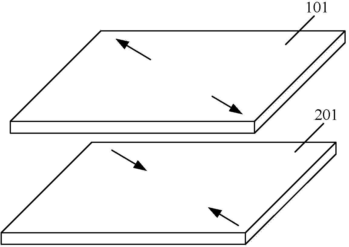
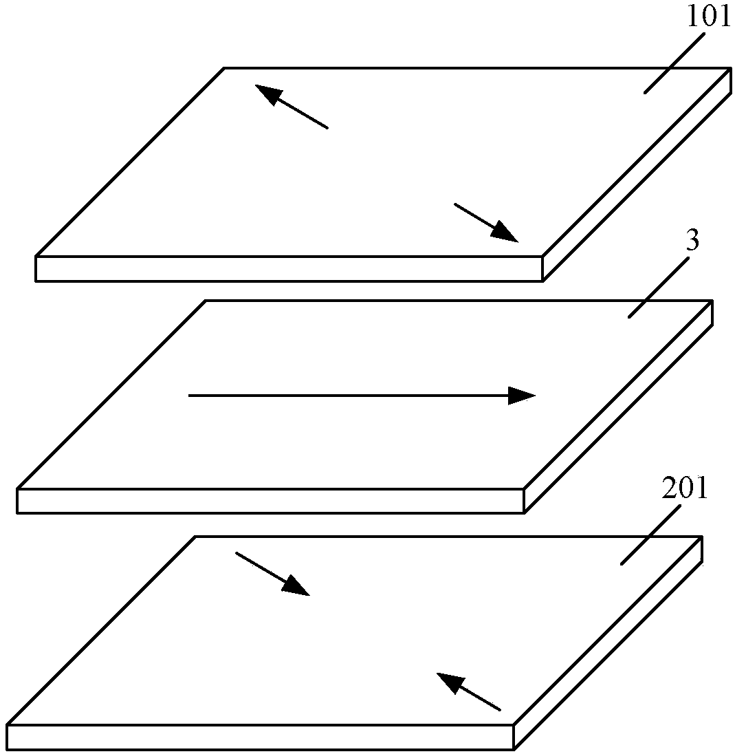
[0036] image 3 A schematic structural diagram of a display substrate provided in Embodiment 1 of the present invention, as shown in image 3 As shown, the display substrate includes a first base substrate 11, a phase delay layer 12 and a first alignment layer 13, the phase delay layer 12 is located above the first base substrate 11, and the first alignment layer 13 is located on the side of the phase delay layer 12. Above, the phase retardation direction of the phase retardation layer 12 is perpendicular to the optical axis direction of the liquid crystal.

[0037] The display substrate may be a color filter substrate. When the display substrate is applied to a display device, the ...


PUM


Abstract

The invention discloses a display substrate, a manufacturing method of the display substrate and a display device. The display substrate comprises a first substrate body, a phase delay layer and a first alignment layer. The phase delay layer is located on the first substrate body. The first alignment layer is located on the phase delay layer. The phase delay direction of the phase delay layer is perpendicular to the optical axis direction of liquid crystals. According to the technical scheme, the phase delay direction of the phase delay layer is perpendicular to the optical axis direction of the liquid crystals, and the phase delay amount generated by the liquid crystals is greatly counteracted, so that the serious dark state light leakage phenomenon is avoided, and the contrast ratio is improved.

Description

technical field [0001] The invention relates to the field of display technology, in particular to a display substrate, a manufacturing method thereof, and a display device. Background technique [0002] For a liquid crystal display (LCD for short), its glass substrate is an isotropic material without phase retardation, so under normal conditions, the liquid crystal display will not produce light leakage. However, when the liquid crystal display is subjected to an external force, the glass substrate will produce anisotropy under pressure, and the direction of the phase retardation produced will be different according to the direction of the force. [0003] The reason for the light leakage in the dark state is explained below by comparing the empty cell and the liquid crystal cell under the action of bending pressure. Figure 1a is a schematic diagram of the phase delay of the empty box under the bending pressure, Figure 1b for Figure 1a Schematic diagram of the light leaka...

Claims


Application Information

Patent Timeline
Patent Type & Authority Applications(China)
IPC IPC(8): G02F1/13363G02F1/1333
CPCG02F1/1333G02F1/13363G02F2413/08G02F1/133565G02F1/133633G02F1/133365G02F1/133512G02F1/133514G02F1/1337G02F2202/022
Inventor 秦广奎
Owner BOE TECH GRP CO LTD
Why Eureka
Try Eureka