Pixel structure and display panel

A pixel structure, pixel electrode technology, applied in nonlinear optics, instruments, optics, etc., can solve the problems of pixel structure storage capacitance drop, overlapping area reduction, serious feed-through voltage, etc., to improve the feed-through voltage problem, low power Consume and increase the effect of storage capacitors

Inactive Publication Date: 2016-01-06
AU OPTRONICS CORP
View PDF5 Cites 0 Cited by
  • Summary
  • Abstract
  • Description
  • Claims
  • Application Information

AI Technical Summary

Problems solved by technology

However, with the improvement of pixel resolution, the unit pixel area is gradually reduced, and the overlapping area between the common electrode and the pixel electrode is also reduced, resulting in a decrease in the storage capacitance of the pixel structure.
As a result, the pixel structure of high-resolution (Pixelperpitch; PPI) products will face the situation that the feedthrough voltage (V-feedthrougheffect) is too serious

Method used


Image

  • Pixel structure and display panel
  • Pixel structure and display panel
  • Pixel structure and display panel

Examples


Embodiment Construction

[0048] The technical solution of the present invention will be described in detail below in conjunction with the accompanying drawings and specific embodiments to further understand the purpose, solution and effect of the present invention, but it is not intended to limit the scope of protection of the appended claims of the present invention.

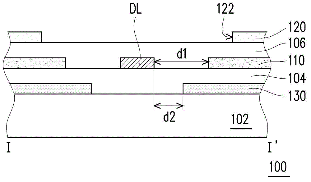
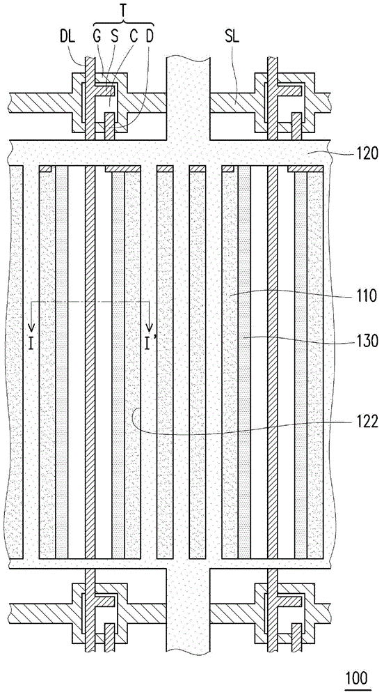
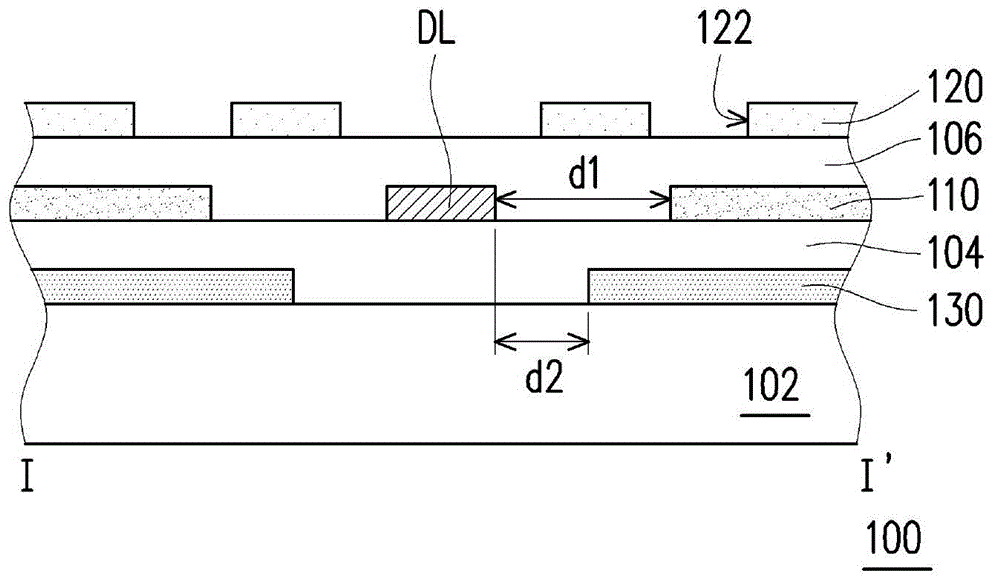
[0049] Figure 1A is a schematic cross-sectional view of a pixel structure according to an embodiment of the present invention, and Figure 1B for Figure 1A An exemplary top view diagram of , where Figure 1A corresponds to Figure 1B The I-I' line. Please also refer to Figure 1A and Figure 1B The pixel structure 100 is disposed on a substrate 102 and includes a data line DL, a scan line SL, an active device T, a pixel electrode 110 , a first common electrode 120 and a second common electrode 130 . The material of the substrate 102 can be glass, quartz, organic polymer, or opaque / reflective material or other applicable materials, ...


PUM


Abstract

The invention relates to a pixel structure and a display panel. The pixel structure is arranged on a substrate and comprises a data line, a scanning line, an active component, a pixel electrode, a first common electrode and a second common electrode. The scanning line and the data line intersect; the active component is electrically connected with the data line and the scanning line; the pixel electrode is electrically connected with the active component; a first projection distance is formed between the pixel electrode and the data line; the first common electrode is disposed on the pixel electrode and overlaps the pixel electrode; the first common electrode comprises a plurality of openings for exposing the pixel electrode; the second common electrode is disposed under the pixel electrode, with the projection thereof overlapping the pixel electrode; a second projection distance is formed between the second common electrode and the data line; and the second projection distance is less than the first projection distance. The display panel with the pixel structure has better display quality and high-resolution products may have lower power consumption.

Description

technical field [0001] The present invention relates to a pixel structure and a display panel, and in particular to a high-resolution pixel structure and a display panel including the pixel structure. Background technique [0002] In recent years, with the maturity of optoelectronic technology and semiconductor manufacturing technology, the flat panel display (FlatPanelDisplay) has been vigorously developed. Liquid crystal displays have replaced traditional cathode ray tube displays due to their advantages of low-voltage operation, no radiation scattering, light weight, and small size, and have become the mainstream of display products in recent years. However, liquid crystal displays still have the problem of limited viewing angles. At present, the technologies that can meet the requirement of wide viewing angle include twisted nematic (twistednematic, TN) liquid crystal plus wide viewing film (wideviewing film), in-plane switching (IPS) liquid crystal display, fringe fiel...

Claims


Application Information

Patent Timeline
Patent Type & Authority Patents(China)
IPC IPC(8): G02F1/1343G02F1/1333
Inventor 张琬珩郑孝威范姜士权
Owner AU OPTRONICS CORP
Why Eureka
Try Eureka