Display device, liquid crystal display panel and manufacturing method of liquid crystal display panel

A liquid crystal panel, liquid crystal technology, applied in nonlinear optics, instruments, optics, etc., can solve the problems of complex manufacturing process and low utilization rate of light energy, simplify the color filter process, reduce light energy loss, and improve the rate of good quality Effect

Active Publication Date: 2015-05-13
BOE TECH GRP CO LTD
View PDF10 Cites 0 Cited by
  • Summary
  • Abstract
  • Description
  • Claims
  • Application Information

AI Technical Summary

Problems solved by technology

[0006] The technical problem to be solved by the present invention is to provide a display device, a liquid crystal panel and a manufacturing method thereof, so as to overcome the problem of depositing a black matrix to cover the position of the gate, source and drain layers in the existing liquid crystal display color filter substrate. The dark state light leakage phenomenon causes defects such as complex manufacturing process and low light energy utilization rate

Method used


Image

  • Display device, liquid crystal display panel and manufacturing method of liquid crystal display panel
  • Display device, liquid crystal display panel and manufacturing method of liquid crystal display panel
  • Display device, liquid crystal display panel and manufacturing method of liquid crystal display panel

Examples


Embodiment Construction

[0026] The specific implementation manners of the present invention will be further described in detail below in conjunction with the accompanying drawings and embodiments. The following examples are used to illustrate the present invention, but are not intended to limit the scope of the present invention.

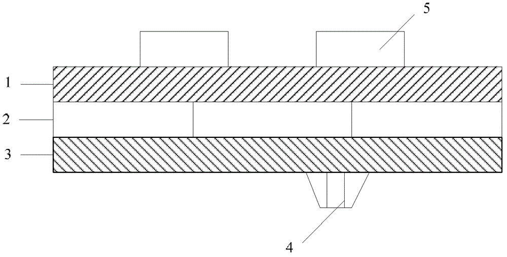
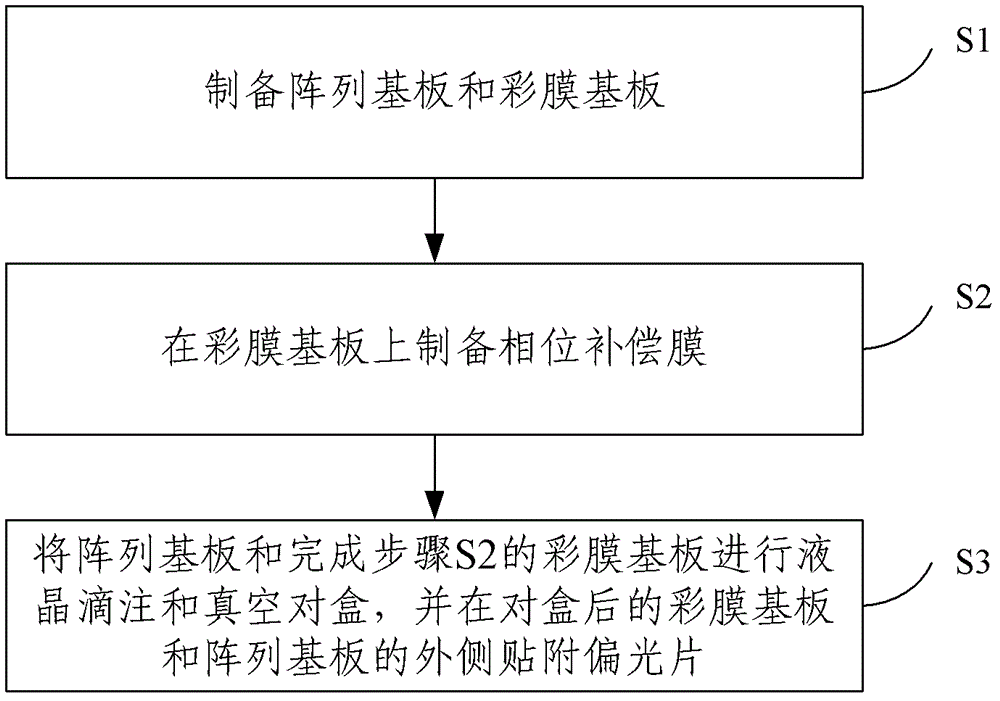
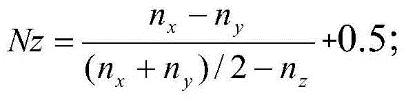
[0027] like figure 1 As shown, the liquid crystal panel provided by the embodiment of the present invention includes: a color filter substrate, an array substrate, a liquid crystal, and a polarizer, the number of polarizers is two, and the two polarizers are respectively arranged on the color filter substrate and the array substrate, wherein , set the polarizer located outside the color filter substrate as the upper polarizer, and the polarizer located outside the array substrate as the lower polarizer. A phase compensation film 5 is provided between the two polarizers.

[0028] The substrate 1 of the color filter substrate has a color pixel layer 2 , a protection layer ...


PUM


Abstract

The invention relates to the technical field of displays, in particular to a display device, a liquid crystal display panel and a manufacturing method of the liquid crystal display panel. The liquid crystal display panel comprises a color film substrate, an array substrate, liquid crystals and polarizers; the two polarizers are respectively arranged on the color film substrate and the array substrate; and a phase compensation film is arranged between the two polarizers. According to the liquid crystal display panel and the manufacturing method thereof, which are provided by the invention, due to the adoption of the phase compensation film, the phenomenon of dark state light leakage caused by deflection of the liquid crystals at the positions of a grid electrode and a source and drain electrode layer due to the generation of irregular terminal differences can be effectively avoided; the design of a black matrix in the color film substrate in the prior art can be canceled by the additionally arranged phase compensation film, so that the color film process program is simplified; and the aperture ratio of a pixel electrode and the light energy utilization rate of backlight can be effectively improved, the light energy loss is furthest reduced and the excellent rate of the product is improved.

Description

technical field [0001] The invention relates to the technical field of displays, in particular to a display device, a liquid crystal panel and a manufacturing method thereof. Background technique [0002] The main structure of TFT-LCD (Thin Film Transistor-Liquid Crystal Display, Thin Film Field Effect Transistor Liquid Crystal Display) is composed of array substrate, color filter substrate, polarizer, backlight and liquid crystal. Among them, the thin film transistor structure is formed by depositing the gate, gate insulating layer, active layer, source layer, drain layer, and pixel electrode layer on the substrate; the black matrix, red, green, and blue pixels, and pixel protection are deposited on the substrate respectively. Layer, common electrode layer and spacers form a color filter substrate. In the vacuum box-to-box process, after the liquid crystal is uniformly dripped on the array substrate or the color filter substrate, the color filter substrate or the array sub...

Claims


Application Information

Patent Timeline
Patent Type & Authority Patents(China)
IPC IPC(8): G02F1/13363G02F1/1333
Inventor 张培林柳在健
Owner BOE TECH GRP CO LTD
Why Eureka
Try Eureka