Group III nitride semiconductor light emitting device
A technology of nitride semiconductors and light-emitting devices, applied in semiconductor devices, electrical components, circuits, etc., can solve the problems of high emission output, reduced possibility of recombination of electrons and holes, and inability to obtain them, and achieve the effect of improving emission intensity
- Summary
- Abstract
- Description
- Claims
- Application Information
AI Technical Summary
Problems solved by technology
Method used
Image

Examples
Embodiment approach 1
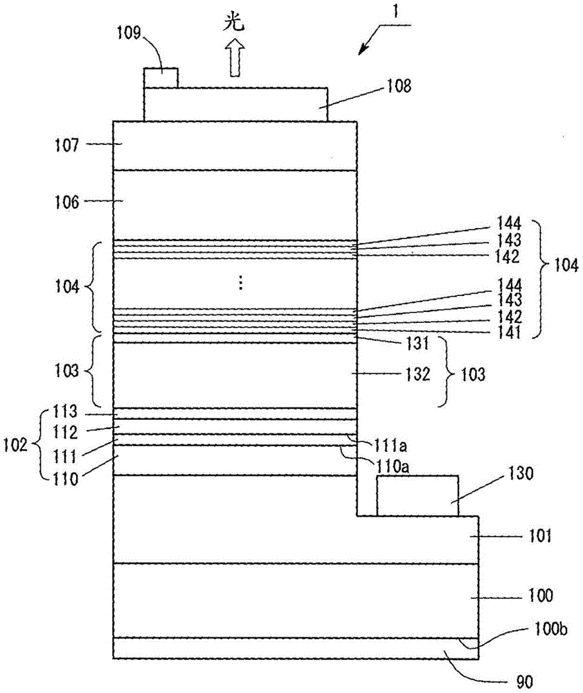
[0038] The light emitting device according to Embodiment 1 has a plurality of Group III nitride semiconductor layers on a GaN substrate having a c-plane main surface.
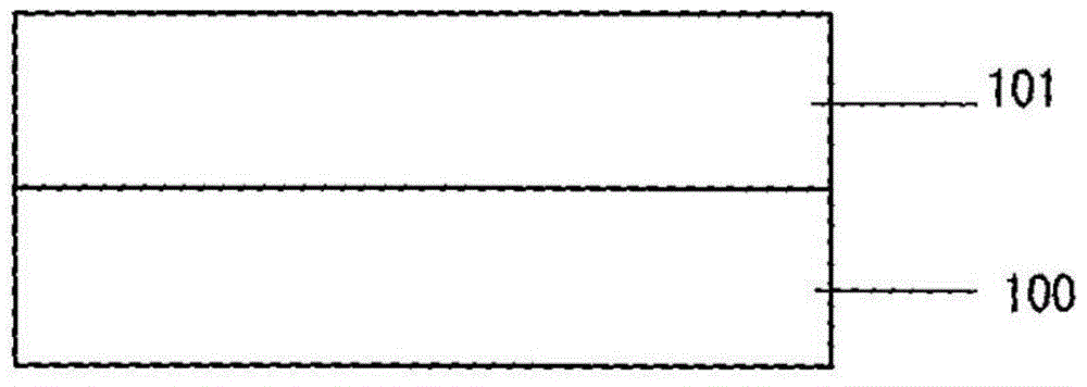
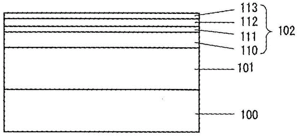
[0039] figure 1 The structure of the light emitting device 1 according to Embodiment 1 is shown. The light emitting device 1 includes: a GaN substrate 100 to which no impurities are added; an n-type contact layer 101; an ESD layer (electrostatic discharge layer) 102; an n-type cladding layer 103; a light-emitting layer 104; 107 , layers 101 to 107 are formed of Group III nitride semiconductors and deposited on a GaN substrate. A p-electrode 108 is formed as a transparent electrode (for example, ITO) on the p-type contact layer 107; a pad electrode 109 is formed at an electrode corner of the p-electrode 108; An n-electrode 130 is formed on a portion of 107 exposed from a corresponding portion of the p-type contact layer 107 etched. An aluminum reflective film 90 is formed on the back surface 100 b of the GaN...
Embodiment approach 2
[0067] The light emitting device 1 according to Embodiment 1 is a face-up type, and the light emitting device 2 according to Embodiment 2 is a face-down type. use with figure 1 The same reference numerals are used to designate elements that play the same role as in Embodiment 1. exist Figure 5 In, the composition is omitted figure 1 Multiple layers of ESD layer 102 and light emitting layer 104 are shown in . The p-electrode 118 to be formed on the entire surface of the p-type contact layer 107 is a reflective film formed of Ni / Al / Ag / Al deposited on the p-type contact layer 107 . The p-electrode 118 also serves as a pad for bonding the light emitting device 2 to the frame. The n-electrode 130 is the same metal stack as in Embodiment 1, and the top surface of the p-electrode 118 and the top surface of the n-electrode 130 are on the same surface, that is, on the same level. Surface 100a of GaN substrate 100 on which no device layer is formed is a light output surface. Th...
Embodiment approach 3
[0069] Figure 6 The light emitting device 3 according to Embodiment 3 shown in is a counter electrode type light emitting device. use with figure 1 The same reference numerals are used to designate elements that play the same role as in Embodiment 1. By using a concentration of 4 x 10 18 / cm 3 Si-doped n-type GaN forms the GaN substrate 100 . N-electrode 140 is formed on the entire surface of back surface 100 b of GaN substrate 100 . The n-electrode 140 is a metal film of Al / Ag / Al sequentially deposited on the back surface 100 b of the GaN substrate 100 . The n-electrode 140 functions as a light reflection film. A p-electrode 128 of ITO is formed on the entire top surface of the p-type contact layer 107 , and a pad electrode 109 is formed at a corner of the p-electrode 128 . In the light emitting device 3 , light is output from the p-type contact layer 107 .
[0070] A light reflection film may be formed on the p-type contact layer 107 , and a transparent n-electrode...
PUM
| Property | Measurement | Unit |
|---|---|---|
| thickness | aaaaa | aaaaa |
| diameter | aaaaa | aaaaa |
| thickness | aaaaa | aaaaa |
Abstract
Description
Claims
Application Information
 - R&D
- Intellectual Property
- Life Sciences
- Materials
- Tech Scout
- Unparalleled Data Quality
- Higher Quality Content
- 60% Fewer Hallucinations
Browse by: Latest US Patents, China's latest patents, Technical Efficacy Thesaurus, Application Domain, Technology Topic, Popular Technical Reports.
© 2025 PatSnap. All rights reserved.Legal|Privacy policy|Modern Slavery Act Transparency Statement|Sitemap|About US| Contact US: help@patsnap.com