

On-chip RAM built-in self-testing method and circuit
A built-in self-test and circuit technology, applied in static memory, instruments, etc., can solve the problems that static faults cannot be fully detected, RAM built-in self-test circuit design is not flexible and efficient, etc., to improve static fault coverage, The effect of improving test efficiency and reducing test cost
- Summary
- Abstract
- Description
- Claims
- Application Information
AI Technical Summary
Problems solved by technology
Method used
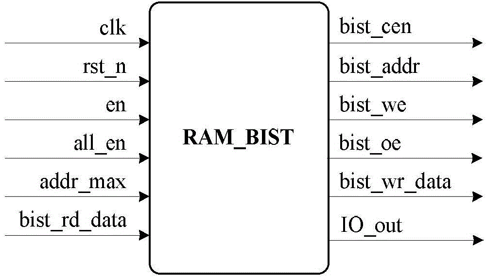
Image

Examples
Embodiment Construction
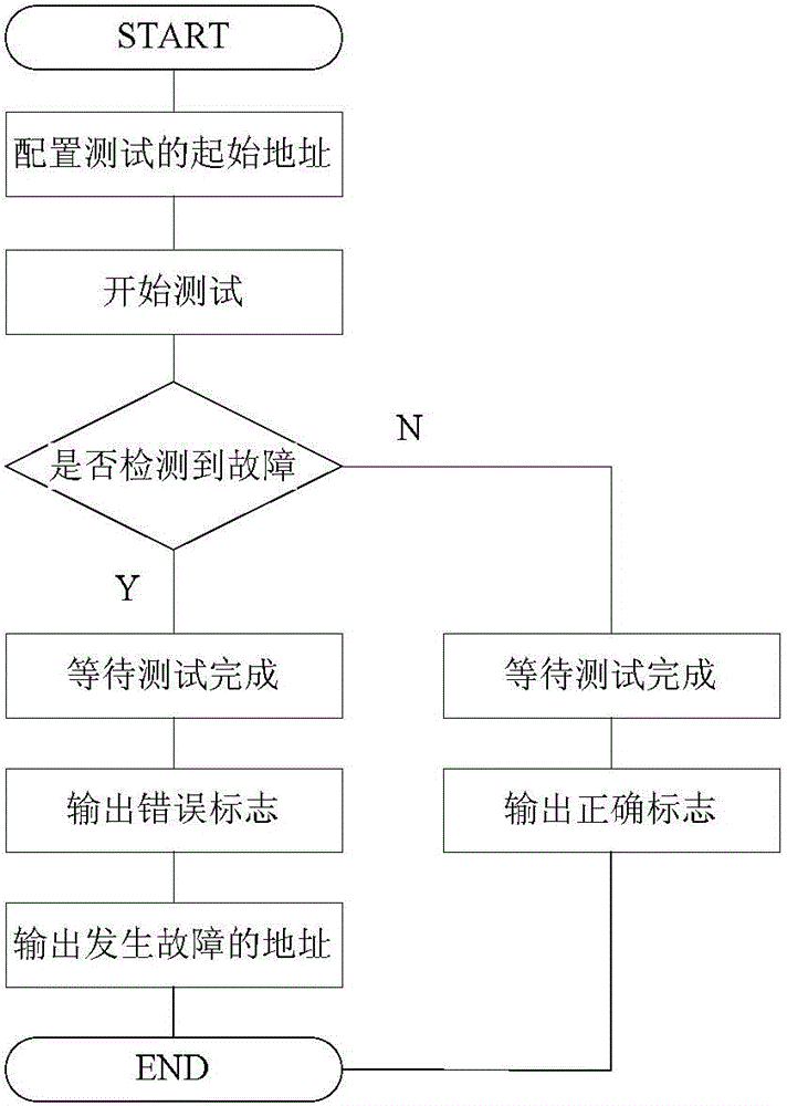
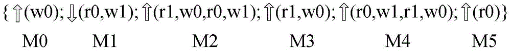
[0026] A preferred embodiment of the present invention provides a kind of on-chip RAM built-in self-test method, comprising the following steps: configure the initial address of the test; start from the initial address, carry out the following operations to each address in the predetermined range: according to the address In ascending order, write 0 operations; in descending order of addresses, perform two read 0 operations and two write 1 operations; in ascending order of addresses, perform read 1 operations, write 0 operations, read 0 operations, and write 1 operations; in ascending order of addresses, perform Two write 1 operations and two read 0 operations; perform read 0, write 1, read 1, and write 0 operations in ascending order of addresses; perform read 0 operations in ascending order of addresses; during the above operations, when a When the read data of a test address is inconsistent with the expected data, it is judged that the test address is faulty, and after the...
PUM
 Abstract
Description
Claims
Application Information