Built-in self testing circuit with fault diagnostic capability

a self-testing circuit and fault technology, applied in the field of semi-conductor integrated circuits, can solve problems such as hard to acquire failure diagnosis information

Inactive Publication Date: 2011-06-14
KK TOSHIBA
View PDF14 Cites 12 Cited by
  • Summary
  • Abstract
  • Description
  • Claims
  • Application Information

AI Technical Summary

Problems solved by technology

In addition, there is a matter in that it is hard to acquire failure diagnosis information which is equivalent to a result of an actual speed test.

Method used


Image

  • Built-in self testing circuit with fault diagnostic capability
  • Built-in self testing circuit with fault diagnostic capability
  • Built-in self testing circuit with fault diagnostic capability

Examples


first embodiment

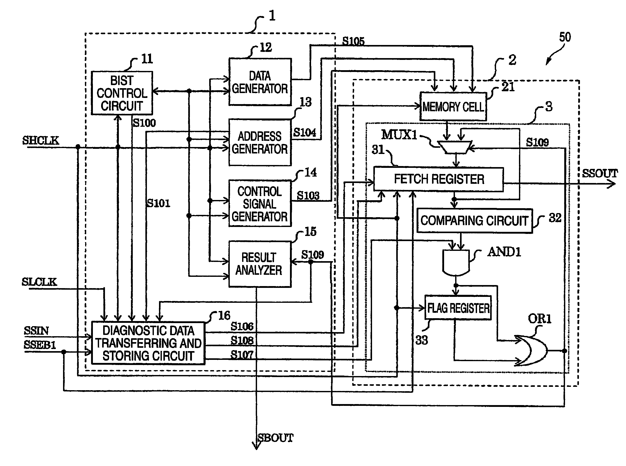
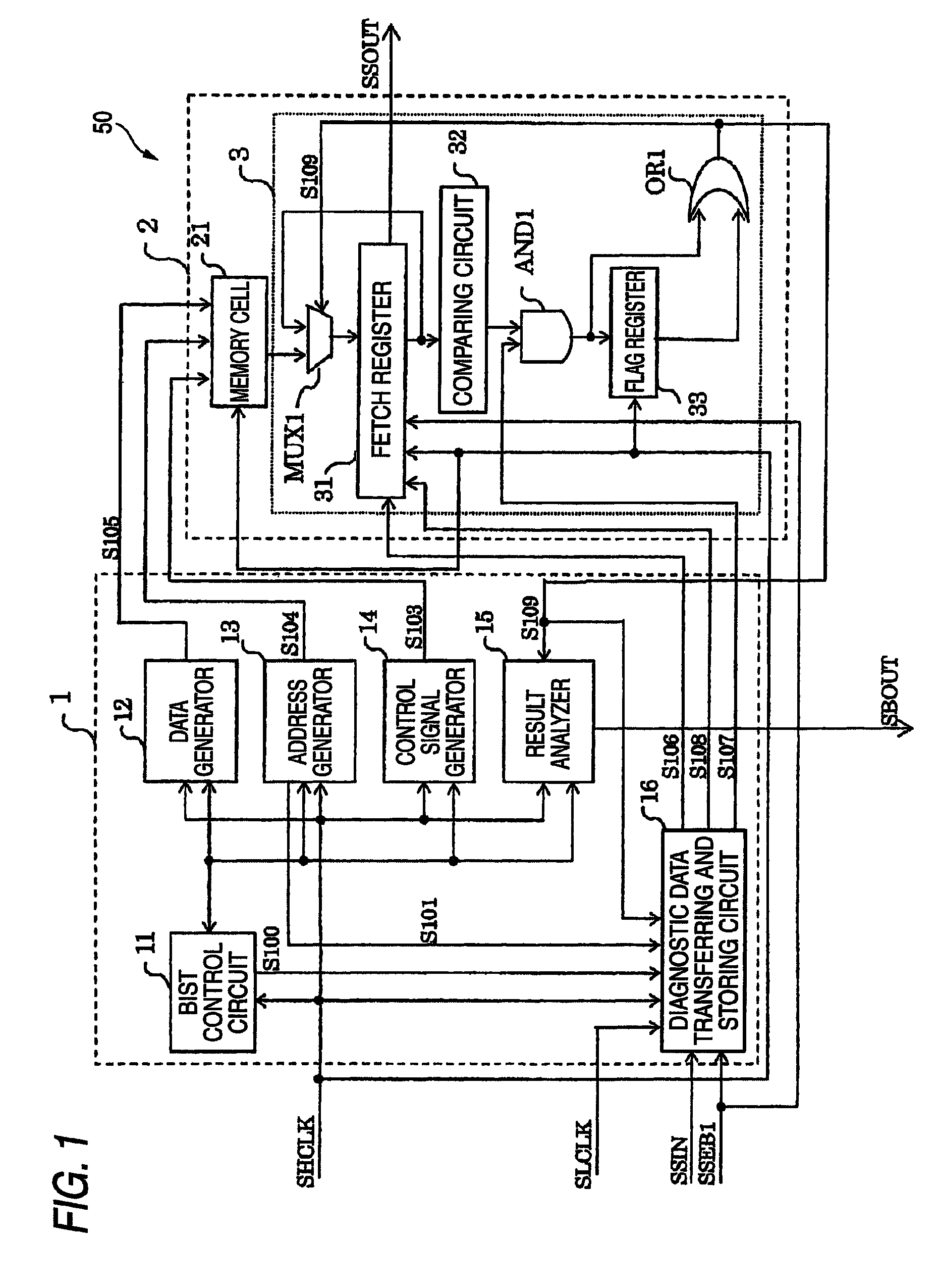
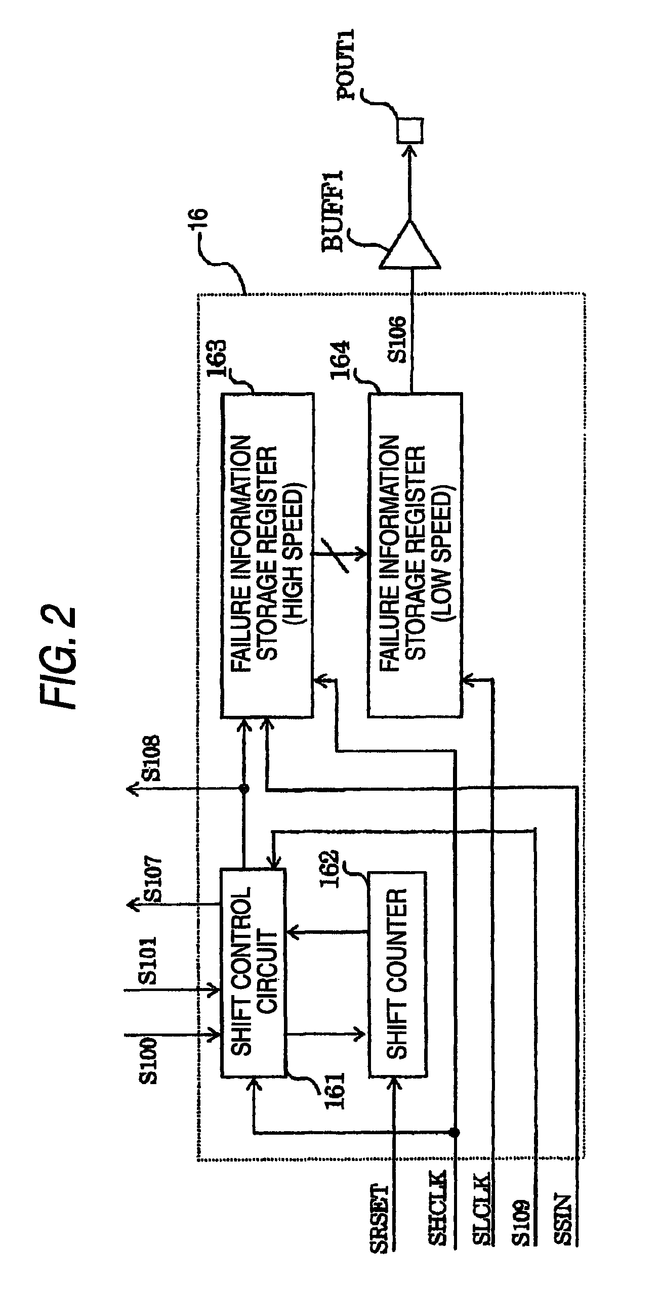
[0015]First of all, a semiconductor integrated circuit according to a first embodiment of the invention will be described with reference to the drawings. FIG. 1 is a block diagram showing a structure of the semiconductor integrated circuit and FIG. 2 is a block diagram showing a structure of a diagnostic data transferring and storing circuit. In the embodiment, the diagnostic data transferring and storing circuit is provided in a BIST circuit.

[0016]As shown in FIG. 1, a semiconductor integrated circuit 50 is provided with a BIST circuit 1 and a memory collar 2. The semiconductor integrated circuit 50 is a system LSI comprising an SRAM (Static Random Access Memory) to be a semiconductor memory, a combinational circuit and a sequential circuit, for example. The memory collar is also referred to as a memory wrapper.

[0017]The BIST circuit 1 is provided with a BIST control circuit 11, a data generator 12, an address generator 13, a control signal generator 14, a result analyzer 15, and a...

second embodiment

[0053]Next, a semiconductor integrated circuit according to a second embodiment of the invention will be described with reference to the drawings. FIG. 4 is a block diagram showing a flow of a signal in the case in which a failure diagnosis for a memory is carried out, and FIG. 5 is a diagram showing a structure of a BIST operation setting register. In the embodiment, a memory other than a failure diagnosing target memory is bypassed to shorten a time required for a data transfer.

[0054]As shown in FIG. 4, a semiconductor integrated circuit 50a is provided with a BIST circuit 1a, a memory collar 401, a memory collar 402, a memory collar 40n, input buffers BUFF11 to BUFF13, an output buffer BUFF21, an output buffer BUFF22, input terminals PIN11 to PIN13, an output terminal POUT11 and an output terminal POUT12. The semiconductor integrated circuit 50a is an SoC (System on a Chip) including an SRAM to be a semiconductor memory, a logic circuit, a sequential circuit and an analog circuit...


PUM


Abstract

A semiconductor integrated circuit includes: a memory collars including: a memory cell; a fetch register that is configured to fetch data as a first fetch data; a comparing unit that is configured to compare the first fetch data with an expected value; a failure detecting signal output unit that is configured to receive the compared result and output a failure detecting signal; and a BIST circuit including: a BIST control unit that is configured to output an instruction and output a BIST status; a shift controller that is configured to receive a first clock signal, the BIST status signal, and the failure detecting signal and output sift enable signal; a shift counter that counts the number of clock pulses on the first clock signal; a first storage register that is configured to receive the first clock signal and the shift enable signal, and a second storage register that is configured to receive a second clock signal.

Description

CROSS-REFERENCE TO RELATED APPLICATIONS[0001]This application claims priority from Japanese Patent Application 2007-227000, filed Aug. 31, 2007, the entire contents of which are incorporated herein by reference.BACKGROUND OF THE INVENTION[0002]1. Technical Field[0003]The present invention relates to a semiconductor integrated circuit and more particularly to a semiconductor integrated circuit for carrying out a failure diagnosing operation by using a built-in self test circuit of a memory.[0004]2. Description of the Related Art[0005]In a semiconductor integrated circuit including a memory, there has been used a technique for incorporating a built-in self test (which will be hereinafter referred to as a BIST), carrying out the BIST by using the BIST circuit to detect a defective chip, and subsequently performing a failure diagnosis over the defective chip by using the BIST circuit, thereby extracting a candidate for a defective portion of the memory. Examples of the BIST circuit incl...

Claims


Application Information

Patent Timeline
Patent Type & Authority Patents(United States)
IPC IPC(8): G01R31/28
CPCG11C29/44
Inventor TOKUNAGA, CHIKAKOANZOU, KENICHI
Owner KK TOSHIBA
Why Eureka
Try Eureka