Shift register circuit and image display apparatus equipped with the same

a register circuit and image display technology, applied in the direction of static storage, digital storage, instruments, etc., can solve the problems of unnecessarily activating the gate line, rewriting the pixel, and displaying defects, so as to achieve the effect of suppressing malfunction

Inactive Publication Date: 2007-11-29
MITSUBISHI ELECTRIC CORP
View PDF0 Cites 207 Cited by
  • Summary
  • Abstract
  • Description
  • Claims
  • Application Information

AI Technical Summary

Benefits of technology

[0028]First object of the present invention is to suppress malfunction caused by leakage current of the constituting transistor and shift in threshold voltage in a...

Problems solved by technology

When the potential of the first node rises by the leakage current and the clock signal, the problem of malfunction arises in which the first transistor that is to be turned OFF is turned ON, and the gate line is unnecessarily activated when the voltage between the gate and the source of the first transistor exceeds a threshold voltage.
When a pixel switch element (active transistor) arranged on each pixel is turned ON, the data in the pixel is re-written, and display defect occurs.
If the turning OFF of the pixel transistor is delayed, the data in the pixel may be re-written on the data of the next line, and display failure may occur.
Furthermore, it is not as simple as with shifting in only one direction since the output signal of the dummy stage may become the wrong start pulse when the shift direction is reversed, if the dummy stage is simply arranged.
Therefore, the drive controlling device of the gate line...

Method used


Image

  • Shift register circuit and image display apparatus equipped with the same
  • Shift register circuit and image display apparatus equipped with the same
  • Shift register circuit and image display apparatus equipped with the same

Examples


first embodiment

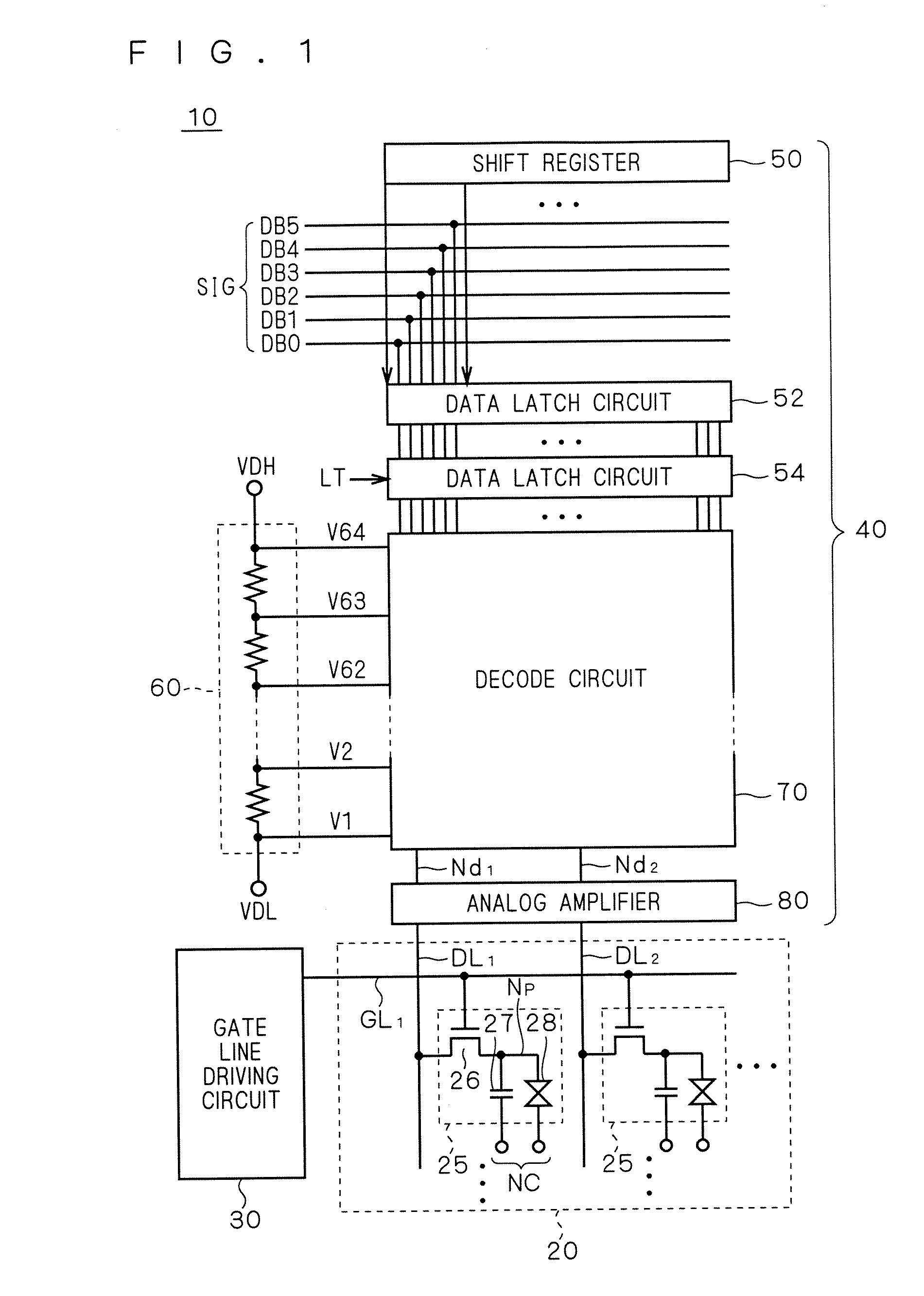
[0067]FIG. 1 is a schematic block diagram showing the configuration of a display apparatus according to a first embodiment of the present invention, showing the entire configuration of a liquid crystal display apparatus 10 as one example of the display apparatus.

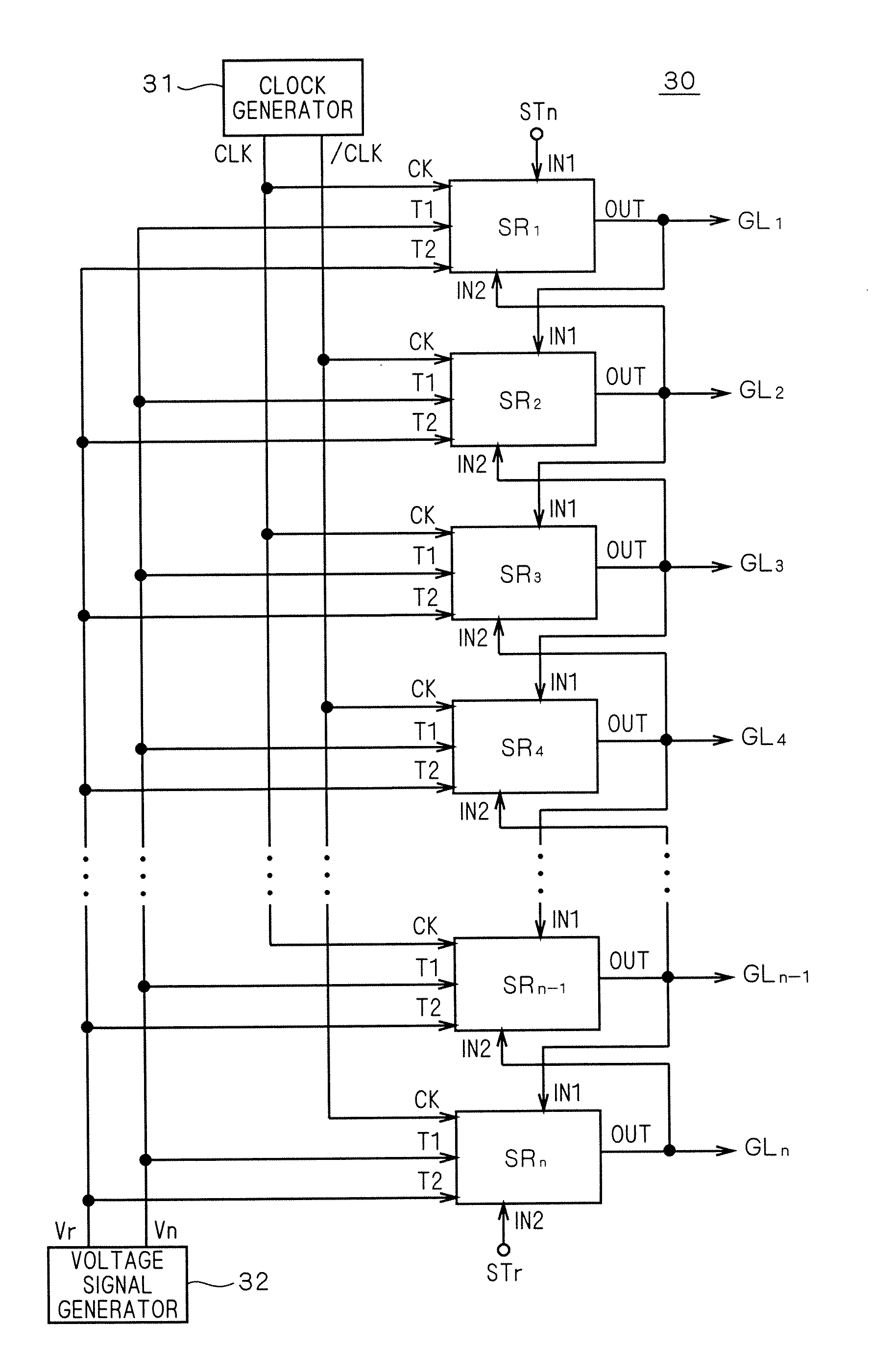
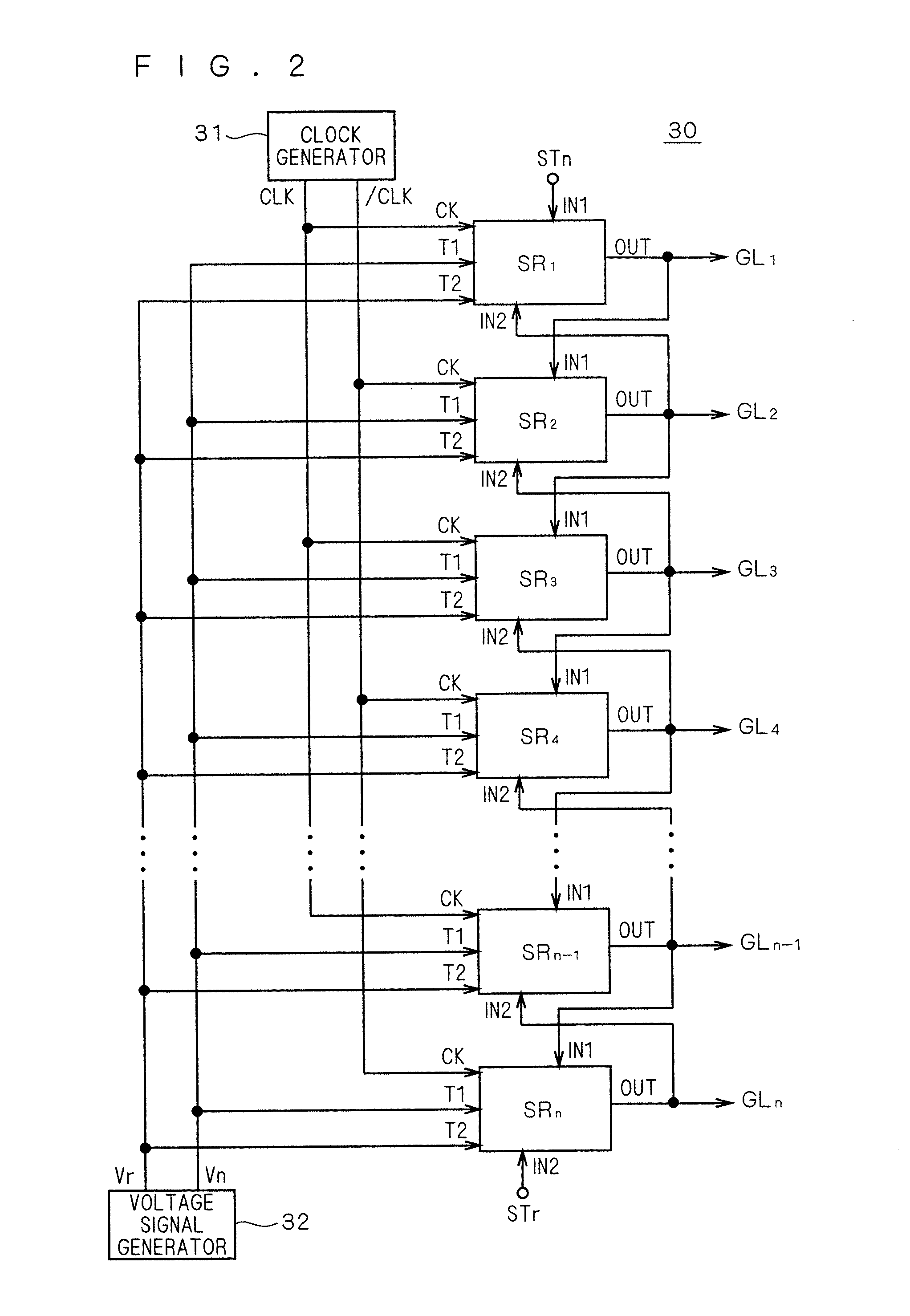
[0068]The liquid crystal display apparatus 10 includes a liquid crystal array section 20, a gate line driving circuit (scanning line driving circuit) 30, and a source driver 40. As to be apparent from the description below, the bi-directional shift register according to the embodiment of the present invention is mounted on the gate line driving circuit 30, and is integrally formed with the liquid crystal array section 20.

[0069]The liquid crystal array section 20 includes a plurality of pixels 25 arranged in a matrix form. The gate lines GL1, GL2, . . . (collectively referred to as “gate line GL”) are arranged on each row of pixels (hereinafter referred to also as “pixel line”), and the data lines DL1, DL2, . . . (collectivel...

second embodiment

[0155]In the bi-directional unit shift register SR configured with a-Si TFT of first embodiment (FIG. 8), since the clock signal / CLK is input to the gate of the transistor Q2, the arise of problem in that the threshold voltage of the transistor Q2 shifts and the driving ability gradually lowers (fourth problem) is suppressed. However, the shift in the threshold voltage of the transistor Q2 is not completely eliminated, and the threshold voltage gradually shifts as the clock signal / CLK repeatedly becomes H level, and the above problem may ultimately arise. In second embodiment, the unit shift register SR capable of further suppressing such problem is proposed.

[0156]FIG. 13 is a circuit diagram showing the configuration of the unit shift register according to second embodiment. As shown in the figure, the source of the transistor Q2 is connected to the first clock terminal CK1. That is, one main electrode (drain) of the transistor Q2 is connected to the output terminal OUT, and the ...

third embodiment

[0160]As described using FIG. 10, when the gate-source voltage VGS(Q5) of the transistor Q5 exceeds the threshold voltage Vth(Q5) in time of rise of the output signal (Gk) in the bi-directional unit shift register SR of first embodiment, the current (I(Q5)) flows from the node N1 to the output terminal OUT via the transistor Q5. As described above, since only slight amount of current normally flows, and thus does not lower the level of the node N1 to an extent of influencing the driving ability of the transistor Q1, the current (I(Q5)) flowing through the transistor Q5 increases and the driving ability of the transistor Q1 may lower when the output load capacity is large and the rise of output signal is slow. The bi-directional unit shift register SR for resolving such problem is proposed in third embodiment.

[0161]FIG. 14 is a circuit diagram of the bi-directional unit shift register SR according to third embodiment. In the unit shift register SR shown in FIG. 14, the gate of the tr...


PUM


Abstract

Malfunction caused by leakage current of the transistor and shift in threshold voltage is prevented in the shift register in which the signal can be shifted bi-directionally. The bi-directional unit shift register includes a first transistor Q1 for providing a first clock signal CLK to an output terminal OUT, a second transistor Q2 for discharging the output terminal OUT based on a second clock signal, third and fourth transistors Q3, Q4 for providing first and second voltage signals Vn, Vr complementary to each other to a first node, which is a gate node of the first transistor Q1, and a fifth transistor Q5 connected between the first node and the output terminal OUT. The fifth transistor Q5 is in an electrically conducted state based on the first clock signal CLK when the gate of the transistor Q1 is at L (Low) level.

Description

BACKGROUND OF THE INVENTION[0001]1. Field of the Invention[0002]The present invention relates to shift register circuits configured only by field effect transistors of the same conductivity type used in scanning line driving circuit and the like of the image display apparatus etc., in particular, to a bi-directional shift register in which the direction of shifting the signal can be reversed.[0003]2. Description of the Background Art[0004]In the image display apparatus (hereinafter referred to as “display apparatus”), such as a liquid crystal display apparatus, a gate line (scanning line) is arranged for each pixel row (pixel line) of a display panel in which a plurality of pixels are arrayed in a matrix form, and the gate line is sequentially selected and driven at a cycle of one horizontal period of the display signal to update the displayed image. A shift register for performing the shift operation that completes the round in one frame period of the display signal is used for the...

Claims


Application Information

Patent Timeline
IPC IPC(8): G11C19/00
CPCG09G3/20G11C19/28G11C19/184G09G3/3677G09G3/36G11C19/00
Inventor TOBITA, YOUICHI
Owner MITSUBISHI ELECTRIC CORP
Why Eureka
Try Eureka