

Semiconductor device and method of manufacturing the same
- Summary
- Abstract
- Description
- Claims
- Application Information
AI Technical Summary
Benefits of technology
Problems solved by technology
Method used
Image

Examples
Embodiment Construction
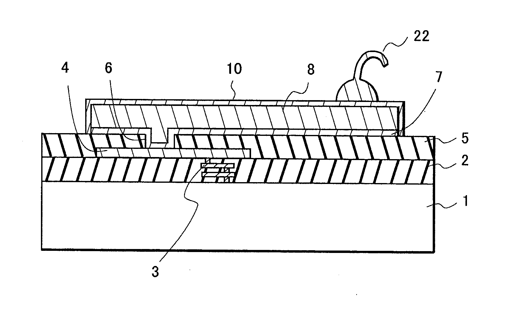
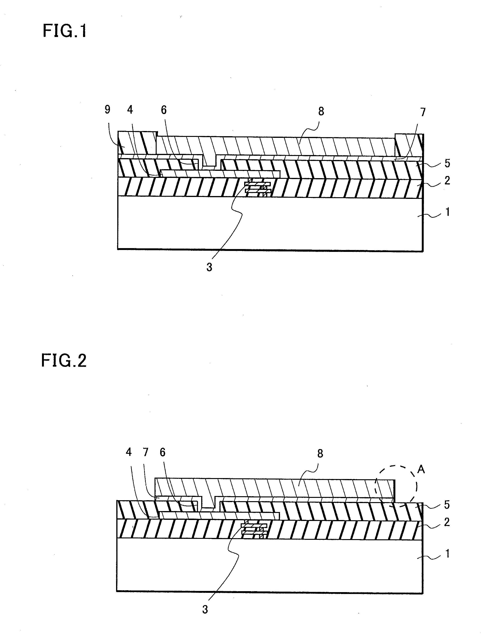
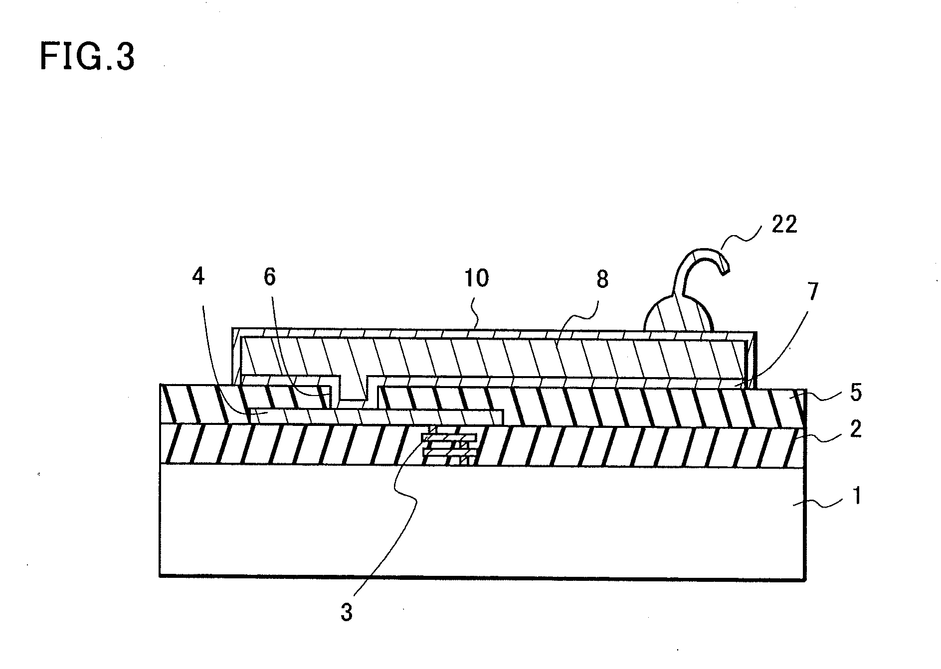
[0030]A description is given of a preferred embodiment of the invention with reference to the drawings.
[0031]In FIGS. 1 to 3, reference numeral 1 denotes a semiconductor substrate formed of, for example, a silicon substrate, and 2 denotes an interlayer insulating film formed on the semiconductor substrate 1. A lower-layer wiring portion 3 connected to a device element is formed in the interlayer insulating film 2. Note that the device element may have a BIP transistor structure or a MOS transistor structure. Any transistor structure may be applied to the device element.
[0032]Reference numeral 4 denotes an upper-layer wiring connected to the lower-layer wiring portion 3, and an insulating film 5 is formed so as to cover the upper-layer wiring 4. Note that each of the lower-layer wiring portion 3 and the upper-layer wiring 4 is formed of a metal film made of, for example, an Al alloy or the like. The insulating film 5 may be formed of, for example, a single layer of a silicon oxide fi...
PUM
 Abstract
Description
Claims
Application Information