Display device and method of driving the same

a technology of display device and drive device, which is applied in the direction of static storage, digital storage, instruments, etc., can solve the problems of affecting the display quality, so as to suppress the increase in power consumption, and remove the residual charge from inside the panel quickly and stably

Active Publication Date: 2015-09-24
SHARP KK
View PDF8 Cites 25 Cited by
  • Summary
  • Abstract
  • Description
  • Claims
  • Application Information

AI Technical Summary

Benefits of technology

[0075]According to the first aspect of the present invention, when electric power supply is shut off in a liquid crystal display device, two processes (the first discharge process and the second discharge process) are performed sequentially for releasing charges from inside the display panel. In the first discharge process, the clock signal potential and the reference potential are set to the first scanning line selection potential. The clock signal potential, which now has the first scanning line selection potential, is supplied to the output node via the output control switching element, bringing each scanning line into selected state. The data signal potential is set to a grounding potential, so a charge in each pixel formation portion is discharged. Also, when power supply is shut off, the first scanning line selection potential changes its level more quickly than the second scanning line selection potential. Therefore, charges on the scanning lines are also discharged in the first discharge process. In the second discharge process, the clear signal potential is set to the second scanning line selection potential. The second scanning line selection potential changes its level more slowly than the first scanning line selection potential when power supply is shut off. Therefore, upon starting the second discharge process, the second scanning line selection potential is kept at a level capable of turning ON the switching element which is included in each bistable circuit. Therefore, charges on the floating nodes in each bistable circuit are discharged in the second discharge process. In addition to the above, each wire which connects the scanning line drive circuit to the drive controller is connected to a discharge unit. Therefore, even if the scanning line selection potential which is supplied to the drive controller becomes lower than a value required for activating the drive controller, thereby causing each output terminal (which is connected to said wire) in the drive controller to come into a high-impedance state, the wire is not brought into a floated state (potential is drawn into the ground potential). Following through the process described above, it is possible to remove residual charge from inside the panel quickly and stably when power supply is shut off.
[0076]According to the second aspect of the present invention, the same advantages as offered by the first aspect of the present invention are offered by utilizing a discharge resistor.
[0077]According to the third aspect of the present invention, the control switch is open at any time other than when power supply is shut off (hereinafter may called “during normal operation”). Therefore, there is no electric current flowing through the discharge resistor. Thus, it is possible to suppress increase in power consumption caused by the discharge resistor during normal operation.
[0078]According to the fourth aspect of the present invention, the control switch is open during normal operation like in the third aspect of the present invention, so there is no electric current flowing through the discharge resistor. Thus, it is possible to suppress increase in power consumption caused by the discharge resistor during normal operation. Also, the control switch is open even at the time of power shutoff until the second scanning line selection potential comes lower than a predetermined value (i.e., a value required for activating the drive controller), so there is no electric current flowing through the discharge resistor. This stabilizes output waveforms from the drive controller until the second scanning line selection potential comes lower than the predetermined value, and therefore makes it possible to remove residual charge from inside the panel even more stably when power is shut off. Also, the fourth aspect provides greater suppression than the third aspect on power consumption increase caused by the discharge resistor at the time of power shut down.
[0079]According to the fifth aspect of the present invention, the wire is not brought to a floating state (since its potential is drawn into the ground potential) even if the second scanning line selection potential becomes lower than a lower operation limit value of the output circuit and the output from the output circuit assumes a high-impedance state. Therefore, it is possible to provide the same advantages as offered by the first aspect of the present invention.
[0080]According to the sixth aspect of the present invention, it becomes possible to draw the potential of the first node into the reference potential at any time in normal operation. Therefore, it is possible to suppress malfunctions.

Problems solved by technology

Although the data signal is sent via the data lines as described above, each data line cannot deliver data signals for a plurality of rows at one time (simultaneously).
Liquid crystal display devices which have such an arrangement as described above may have a problem that even if the user has shut off power supply, the display is not cleared immediately, with an image persisting like a residual image.
If power supply to the device is turned on while there is a residual charge stored in the pixel formation portion, the residual charge may lower display quality with flickers for example, by causing uneven distribution of impurities.
In the gate driver monolithic panel, it is impossible to employ the above-described method in regard to releasing the charge from the panel.

Method used


Image

  • Display device and method of driving the same
  • Display device and method of driving the same
  • Display device and method of driving the same

Examples


first embodiment

1. First Embodiment

[0106]

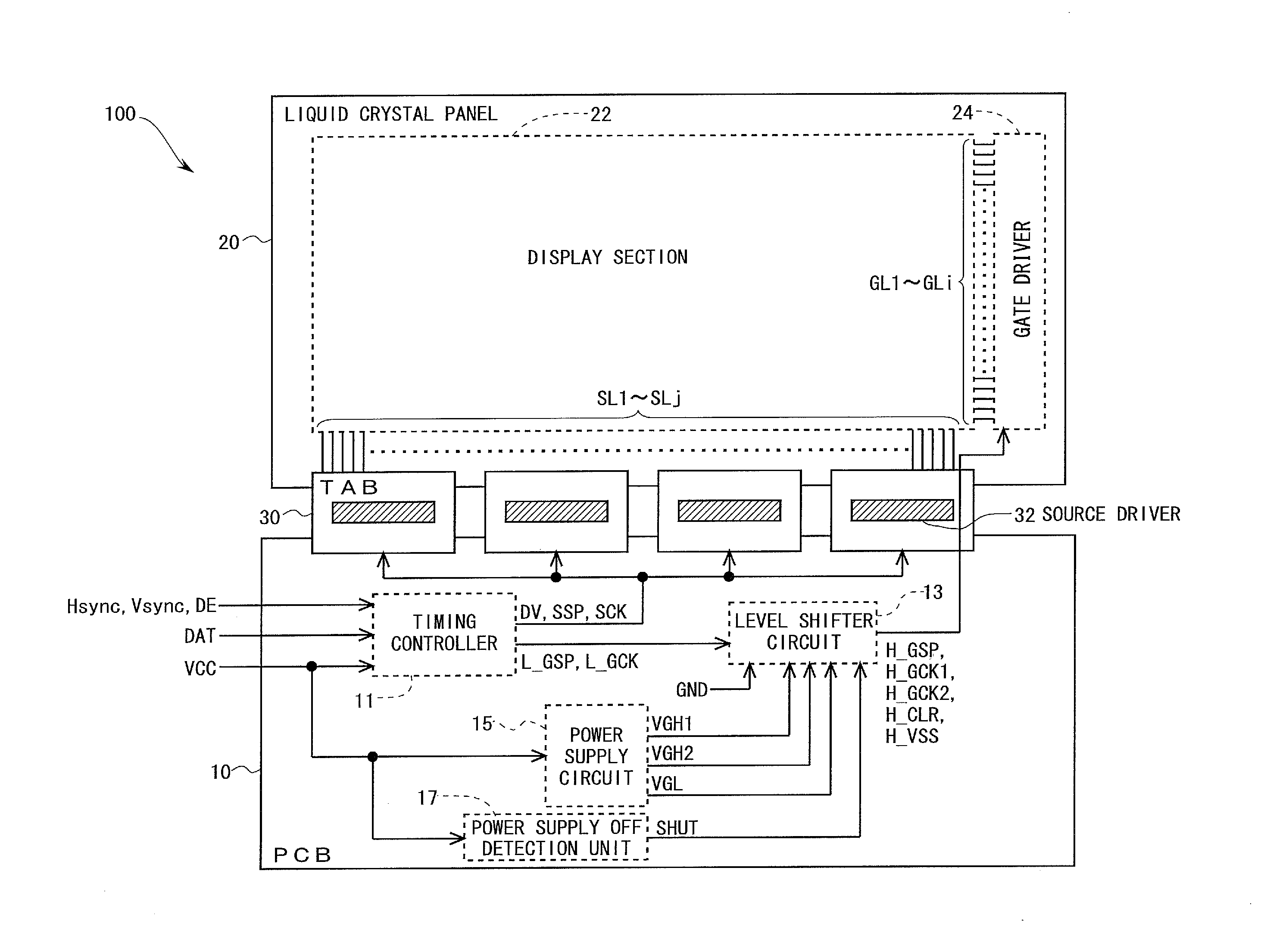
[0107]FIG. 1 is a block diagram which shows an overall configuration of an active matrix liquid crystal display device 100 according to the present embodiment. The liquid crystal display device 100 includes a printed circuit substrate (PCB) 10, a liquid crystal panel 20 as a display panel, and a tape automated bonding (TAB) tape 30 connected to the PCB 10 and the liquid crystal panel 20. The PCB 10 is provided with a timing controller 11, a level shifter circuit 13, a power supply circuit 15, and a power supply OFF detection unit 17. Further, the PCB 10 is also provided with an unillustrated discharge unit which will be described later, but this will not be covered while reference is made to FIG. 1. The liquid crystal panel 20 is provided by an IGZO-TFT liquid crystal panel. The TAB tape 30 is mounted with a source driver 32 in the form of an IC chip, for driving data lines SL1 through SLm. The TAB tape 30 is a package form of the source driver 32 utilized m...

second embodiment

2. Second Embodiment

[0176]

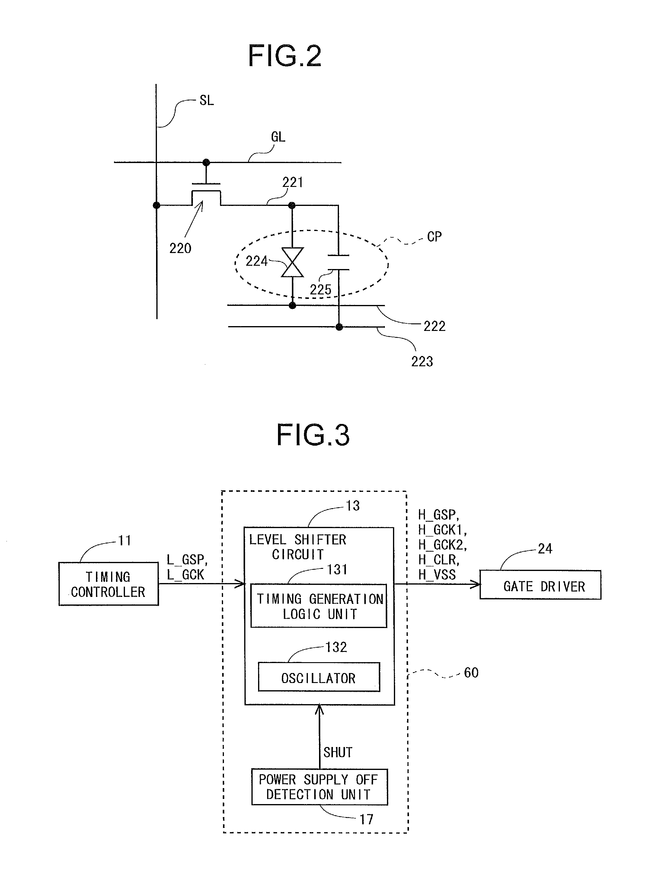
[0177]FIG. 14 is a block diagram for describing a configuration of a discharge unit 190 in a second embodiment according to the present invention. Constituent elements of the present embodiment which are identical with those in the first embodiment will be indicated by the same reference symbols, without repeating description thereof when appropriate. In the present embodiment, the discharge unit 190 includes a control switch 192 in series with the discharge resistor 191, in addition to the discharge resistor 191. In the present embodiment, the control switch 192 is between the discharge resistor 191 and a grounding line (see FIG. 14); however, it maybe between the discharge resistor 191 and the wire OL. The control switch 192 is controlled based on a control signal DIS. The control signal DIS is generated by the level shifter circuit 13 for example. The control switch 192 opens when the control signal DIS is at HIGH level, i.e., the switch electrically sep...

third embodiment

3. Third Embodiment

[0182]

[0183]FIG. 16 is a timing chart for describing a normal operation and an operation upon power shut down in the present embodiment. Constituent elements of the present embodiment which are identical with those in the first and second embodiments will be indicated by the same reference symbols, without repeating description thereof when appropriate. In the present embodiment, the discharge unit 190 is identical with the one in the second embodiment in its configuration. Referring to FIG. 16, assume that the second gate-on potential VGH2 is lower than the lower operation limit value at Time Point t3a. In the present embodiment, the control signal DIS assumes HIGH level when the second gate-on potential VGH2 is not lower than the lower operation limit value, while assuming LOW level when the second gate-on potential VGH2 is lower than the lower operation limit value. Thus, when the second gate-on potential VGH2 is not lower than the lower operation limit value (...


PUM


Abstract

A gate driver (24) which is provided by an IGZO-GDM and a level shifter circuit (13) are connected to each other via a first through a fifth wires (OL1 through OL5). Each wire (OL) is connected to a discharge unit (190). If an electric power supply to a first through a fifth output circuits (OC1 through OC5) in the level shifter circuit (13) becomes lower than a lower operation limit value during a power-off sequence which is supposed to remove a residual charge from inside a panel, outputs from the first through the fifth output circuits (OC1 through OC5) assume a high-impedance state, whereupon a potential on each wire (OL) is drawn by a discharge unit (190) into a ground potential. Therefore, residual charge inside the panel is removed quickly and stably when power supply is shut off.

Description

TECHNICAL FIELD[0001]The present invention relates to display devices and methods of driving the same.BACKGROUND ART[0002]Typically, an active-matrix liquid crystal display device includes a liquid crystal panel constituted by a liquid crystal layer and two substrates which sandwich the liquid crystal layer. One of these two substrates is formed with a plurality of scanning lines, a plurality of data lines, and a plurality of pixel formation portions arranged in a matrix pattern, with each portion formed correspondingly to one of intersections made by the these scanning lines and the data lines. Each pixel formation portion includes such components as: a thin film transistor (TFT) which has its gate terminal connected to one of the scanning lines that passes a corresponding one of the intersections, and its source terminal connected to one of data lines that passes that intersection; and a pixel capacitance for writing a data signal sent via the data line. The other of the two subst...

Claims


Application Information

Patent Timeline
Patent Type & Authority Applications(United States)
IPC IPC(8): G09G3/36
CPCG09G3/3688G09G2300/0876G09G2300/0819G09G2330/021G09G3/3648G09G3/3677G09G3/3696G09G2310/0251G09G2310/0286G09G2330/02G09G2330/027G11C19/28
Inventor IWAMOTO, AKIHISAOZAKI, MASAMINISHIMURA, TOMOHIKOSAITOH, KOHJIUEHATA, MASAKINAKATA, JUN
Owner SHARP KK
Why Eureka
Try Eureka