Substrate structure and method for forming monolithic photodetection and electrical signal processing integrated device

A technology of integrated devices and photodetectors, applied in the direction of electrical components, semiconductor devices, circuits, etc., can solve problems such as the lack of monolithic integration solutions, and achieve the effect of solving the problem of monolithic integration of electronic devices

Active Publication Date: 2017-01-04
UNITED MICROELECTRONICS CENT CO LTD
View PDF3 Cites 0 Cited by
  • Summary
  • Abstract
  • Description
  • Claims
  • Application Information

AI Technical Summary

Problems solved by technology

[0005] In view of this, the object of the present invention is to provide a substrate structure and its formation method for monolithic photodetection and electrical signal processing integrated devices. Disadvantages of separate processing of detection signals and lack of monolithic integrated solutions

Method used


Image

  • Substrate structure and method for forming monolithic photodetection and electrical signal processing integrated device
  • Substrate structure and method for forming monolithic photodetection and electrical signal processing integrated device
  • Substrate structure and method for forming monolithic photodetection and electrical signal processing integrated device

Examples


Embodiment Construction

[0030] The preferred embodiments of the present invention will be described in detail below with reference to the accompanying drawings.

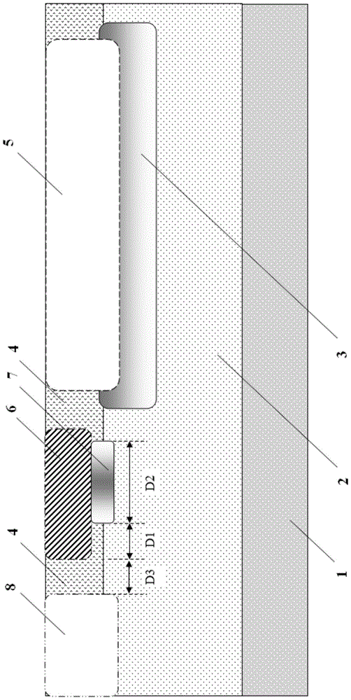
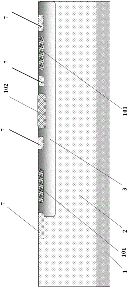
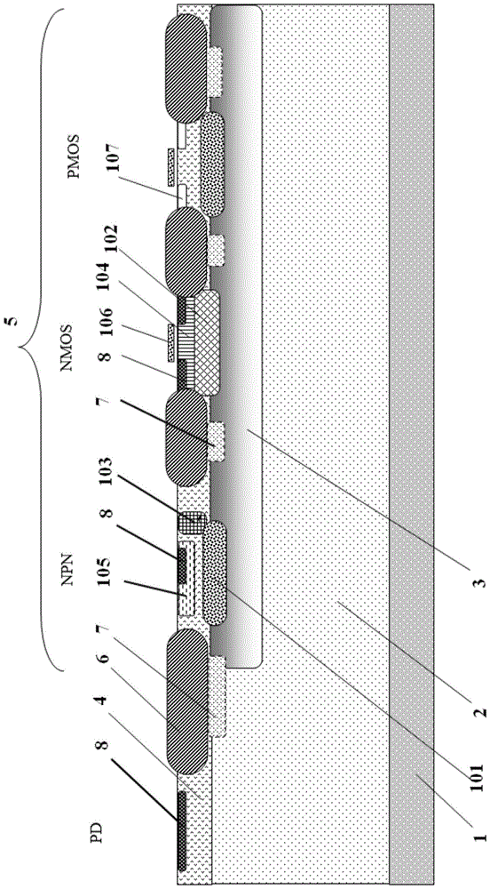
[0031] figure 1 It is a schematic diagram of the substrate structure for a monolithic optical detection and electrical signal processing integrated device. The substrate structure for a monolithic optical detection and electrical signal processing integrated device according to the present invention includes a low-resistance semiconductor material 1, a high-resistance semiconductor Material 2, depletion suppression region 3, device epitaxial layer 4, electronic device region 5, photoelectric isolation dielectric region 6, photoelectric isolation channel blocking region 7 and photodetector ohmic contact region 8;

[0032] The photoelectric isolation dielectric region 6 is connected to the photoelectric isolation channel blocking region 7, and the device epitaxial layer 4 is isolated; the distance D1 between the left side of the photoelectric...


PUM


Abstract

The invention relates to a substrate structure for a monolithic optical detection and electric signal processing integrated device and a forming method of the substrate structure, and belongs to the technical field of semiconductor devices and integrated circuits. According to the scheme, under the condition of high-resistance silicon semiconductor material optical detection and optical detection signal separated processing and lack of a monolithic integration solution, the problems that the difference of the work voltage of an optical detector and the work voltage of an optical detecting signal processing circuit is large, and an optical detecting device structure and an optical detecting signal processing circuit device structure can be hardly compatible with a process can be solved. According to the scheme, the integrated electronic device can comprise an independent NPN transistor, an NMOS transistor, a PMOS transistor, a DMOS transistor or the combination of the independent NPN transistor, the NMOS transistor, the PMOS transistor and the DMOS transistor. According to the scheme, the substrate structure comprises eight basic structure elements, namely, a low-resistance semiconductor material (1), a high-resistance semiconductor material (2), an exhaust restraining area (3), a device epitaxial layer (4), an electronic device area (5), an optoelectronic isolation dielectric area (6), an optoelectronic isolation channel blocking area (7) and an optical detector ohmic contact area (8).

Description

technical field [0001] The invention belongs to the technical field of semiconductor devices and integrated circuits, and relates to a base material structure and a forming method for monolithic optical detection and electrical signal processing integrated devices. Background technique [0002] There are many types of existing photodetection semiconductor devices from the perspectives of spectral response, device structure, and working mode. From the perspective of spectrum, it can respond to light waves with a wavelength of 300nm to 4500nm; from the perspective of semiconductor materials, there can be compound semiconductors and elemental semiconductors; from the perspective of device structure and manufacturing process, most of the relatively mature and variety of elemental silicon semiconductor devices are visible light Detectors, and most of them are based on the improvement of commercial CMOS technology; from the application point of view, the vast majority of photodete...

Claims


Application Information

Patent Timeline
Patent Type & Authority Patents(China)
IPC IPC(8): H01L31/0352H01L31/101H01L31/18
CPCH01L31/035272H01L31/101H01L31/18Y02P70/50
Inventor 谭开洲谭千里黄绍春李荣强黄文刚张兴季万涛王健安杨永晖鲁卿高传顺但伟王品红
Owner UNITED MICROELECTRONICS CENT CO LTD
Why Eureka
Try Eureka