Array substrate, display panel, manufacturing method, and display device

A technology for array substrates and display panels, which is applied to optics, instruments, electrical components, etc., can solve problems such as damage, and achieve the effect of reducing the possibility and display abnormalities

Active Publication Date: 2017-10-20
HEFEI XINSHENG OPTOELECTRONICS TECH CO LTD +1
View PDF5 Cites 0 Cited by
  • Summary
  • Abstract
  • Description
  • Claims
  • Application Information

AI Technical Summary

Problems solved by technology

[0005] In view of this, the present invention provides an array substrate, a display panel, a manufacturing method, and a display device, so as to solve the problem that the existing PLG wiring is easy to cause damage

Method used


Image

  • Array substrate, display panel, manufacturing method, and display device
  • Array substrate, display panel, manufacturing method, and display device
  • Array substrate, display panel, manufacturing method, and display device

Examples


Embodiment Construction

[0049] In order to make the technical problems, technical solutions and advantages to be solved by the present invention clearer, the following will describe in detail with reference to the drawings and specific embodiments.

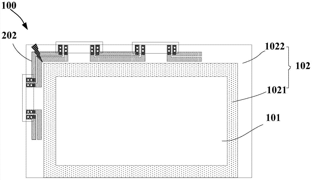
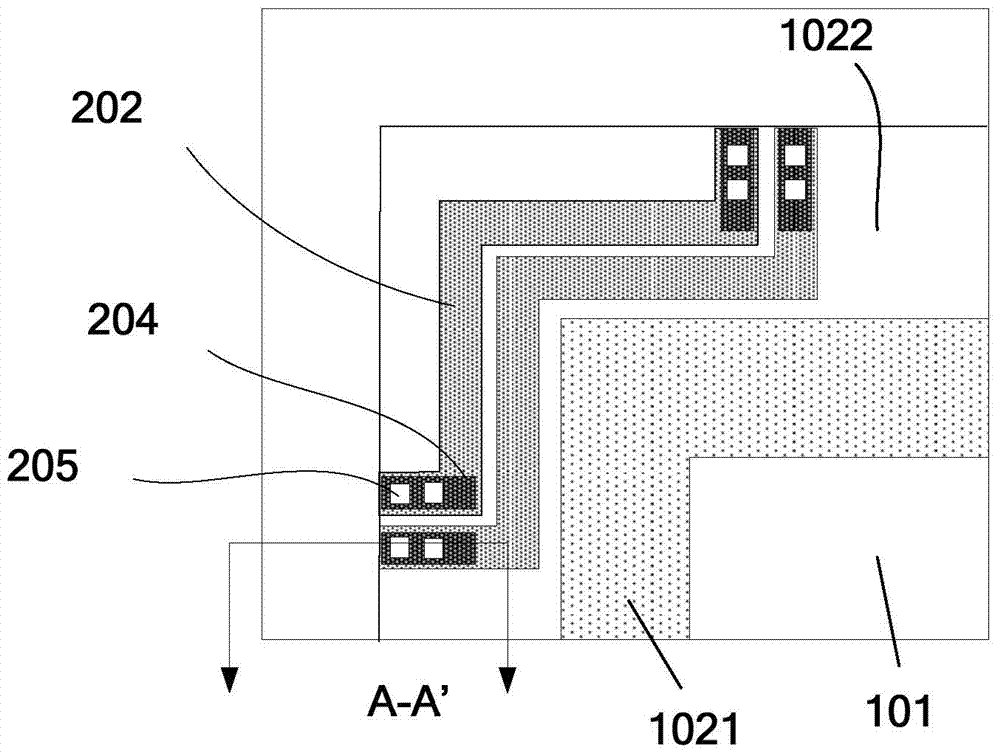
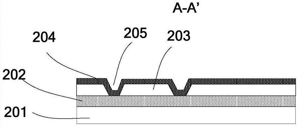
[0050] Please refer to Figure 4 , Figure 4It is a schematic structural diagram of an array substrate according to Embodiment 1 of the present invention. The array substrate includes: a display area 101 and a non-display area 102. The non-display area 102 includes a sealant area 1021 located on the periphery of the display area 101 and a The peripheral area 1022 on the periphery of the sealant area 1021 . Wherein, the sealant area 1021 is used for setting the sealant, so as to box the array substrate and a color filter substrate. The array substrate further includes: a plurality of signal connection lines for connecting the drive unit 400, the signal connection lines include a first connection line 301, a part of the first connection line 301 is locat...


PUM


Abstract

The present disclosure provides an array substrate, a display panel, manufacturing methods thereof and a display device. The array substrate includes a display region and a non-display region. The non-display region includes a sealant region arranged at a periphery of the display region and a peripheral region arranged at a periphery of the sealant region. The array substrate further includes a plurality of signal connection lines for connecting driving lines. The signal connection lines include a first connection line, a portion of which is arranged at the peripheral region and another portion of which is arranged at the sealant region.

Description

technical field [0001] The present invention relates to the field of display technology, in particular to an array substrate, a display panel, a preparation method, and a display device. Background technique [0002] TFT-LCD (Thin Film Transistor Liquid Crystal Display) mainly includes a color filter (CF) substrate, an array (Array) substrate, and liquid crystal filled between the two substrates. At the same time, the sealant can also seal the liquid crystal between the two substrates. Usually, the array substrate is slightly larger than the color filter substrate, and the extra part mainly leaves space for the bonding of the gate drive unit (Gate IC) and the source drive unit (Source IC). [0003] Please refer to Figure 1 to Figure 3 , figure 1 is a schematic structural diagram of an existing array substrate, figure 2 for figure 1 The enlarged view of the corner of the array substrate in ; image 3 for figure 2 Sectional view of plane A-A' in . [0004] From f...

Claims


Application Information

Patent Timeline
Patent Type & Authority Patents(China)
IPC IPC(8): G02F1/13G02F1/1362G02F1/1339G02F1/1333
CPCG02F1/1333G02F1/136286G02F1/136295G02F1/1339G02F1/1345G02F2201/123G02F1/133514G02F2201/121H01L27/124H01L27/1262
Inventor 蒋学兵林琳
Owner HEFEI XINSHENG OPTOELECTRONICS TECH CO LTD
Why Eureka
Try Eureka