Fingerprint sensing device and electronic equipment
A technology for sensing devices and fingerprints, applied in the direction of acquiring/arranging fingerprints/palmprints, instruments, characters and pattern recognition, etc., can solve problems such as wear and tear of fingerprint sensing devices, and achieve the effect of improving service life
- Summary
- Abstract
- Description
- Claims
- Application Information
AI Technical Summary
Problems solved by technology
Method used
Image

Examples
Embodiment 1
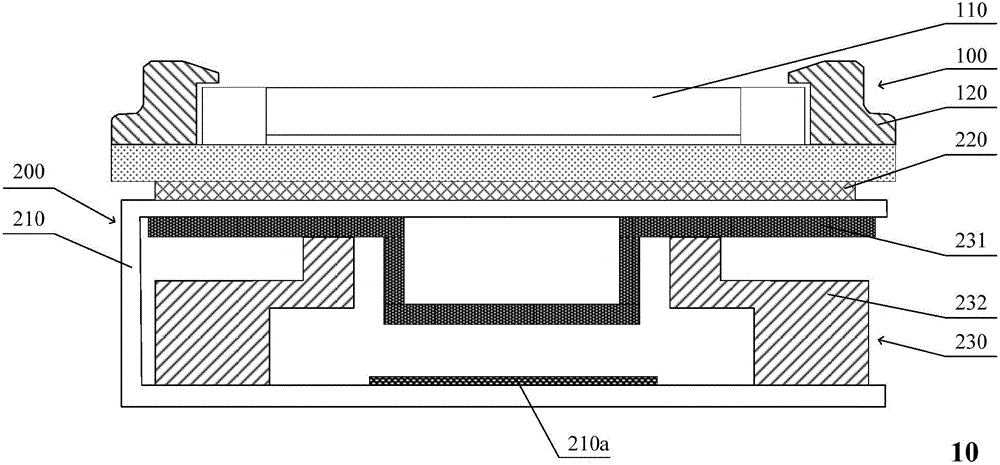
[0036] figure 1 It is a schematic structural diagram of a fingerprint sensing device provided by Embodiment 1 of the present invention. Such as figure 1 As shown, the fingerprint sensing device 10 includes: a panel assembly 100 and a fingerprint identification module 200 arranged below the panel assembly 100; the fingerprint identification module 200 includes a flexible element 210 and a fingerprint identification circuit arranged above the flexible element 210 220, a switch module 230 is nested inside the flexible element 210, and the switch module 230 includes a support 231 in contact with the upper top of the flexible element 210 and a non-conductive elastic element 232 located below the support 231, the support The inside of the part 231 and the non-conductive elastic element 232 forms a conductive boss, which is used to conduct the pad circuit 210a at the bottom of the flexible element 210 when the fingerprint sensing device 10 is pressed, through the opening of the swit...
Embodiment 2
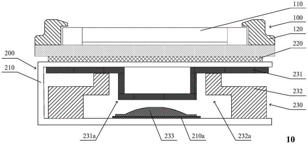
[0046] figure 2 It is a schematic structural diagram of another fingerprint sensing device provided by an embodiment of the present invention. The fingerprint sensing device 10 provided by this embodiment is described above figure 1 On the basis of the illustrated embodiment, a specific structure of the switch module 230 is shown, wherein a first concave platform 232a is arranged in the middle of the non-conductive elastic element 232 in the switch module 230, and the inside of the first concave platform 232a A through hole is provided, and a first boss 231a protruding downward is arranged in the middle of the support member 231 above the non-conductive elastic element 232, and the first boss 231a is nested in the first recess 232a and passes through the In the through hole of the first concave platform 232a, an upwardly protruding metal dome 233 is provided above the pad circuit 210a, and the first convex platform 231a of the support member 231 is used for downward displace...
Embodiment 3
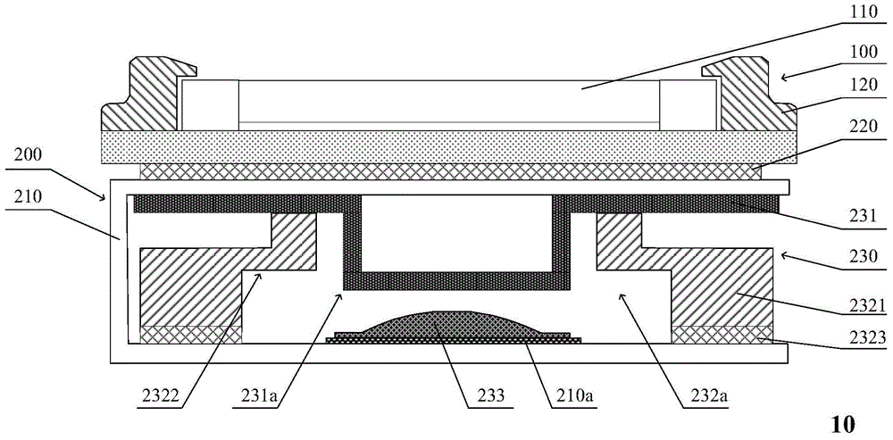
[0054] Figure 4 It is a schematic structural diagram of a fingerprint sensing device provided by Embodiment 3 of the present invention. Such as Figure 4 shown in the above figure 1 Based on the structure of the fingerprint sensing device provided in the illustrated embodiment, in the fingerprint sensing device 10 provided in this embodiment, the switch module 230 also includes a support member 231 and a non-conductive elastic element 232. The difference is that the figure 1 The supporting member 231 and the non-conductive elastic element 232 are replaced with the following structure, specifically, the non-conductive elastic element 232 is provided with a downwardly protruding second boss 232b, and the bottom of the second boss 232b is provided with conductive particles 234 The conductive particles 234 are used to contact the pad circuit 210a at the bottom of the flexible element 210 when the fingerprint sensing device 10 is pressed, and the flexible element 210 is turned o...
PUM
 Abstract
Description
Claims
Application Information
 - R&D Engineer
- R&D Manager
- IP Professional
- Industry Leading Data Capabilities
- Powerful AI technology
- Patent DNA Extraction
Browse by: Latest US Patents, China's latest patents, Technical Efficacy Thesaurus, Application Domain, Technology Topic.
© 2024 PatSnap. All rights reserved.Legal|Privacy policy|Modern Slavery Act Transparency Statement|Sitemap