

Strained sigesn fin photodetector
A photodetector, fin-type technology, applied in circuits, electrical components, semiconductor devices, etc., can solve problems such as deterioration of material quality and thermal stability, difficulty in preparing high-quality GeSn, and difficulty in wide-ranging band gap adjustment. To achieve the effect of low material, low cost, and improved adjustment effect
- Summary
- Abstract
- Description
- Claims
- Application Information
AI Technical Summary
Problems solved by technology
Method used
Image

Examples
Embodiment 1
[0024] Embodiment 1, the strained SiGeSn fin photodetector of double-layer structure absorption region, single-layer structure stress layer
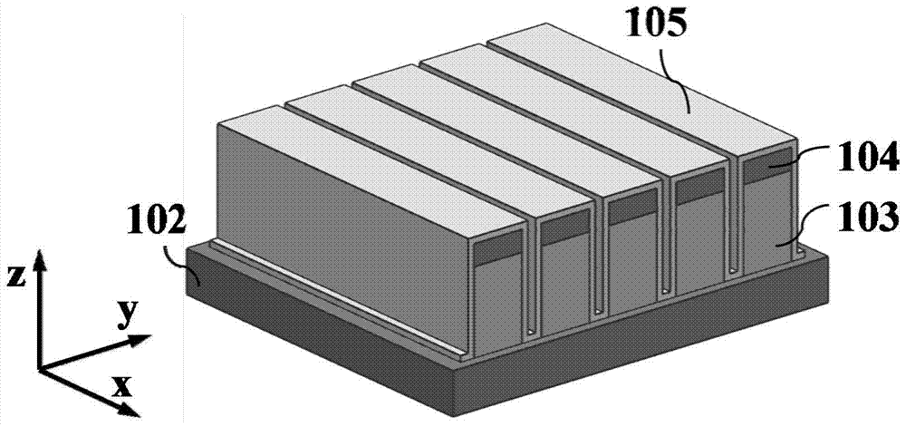
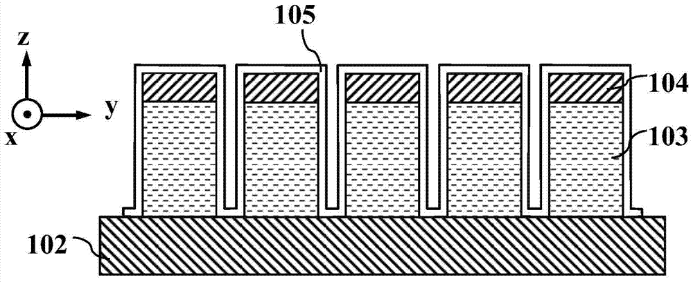
[0025] refer to figure 1 , this example includes from bottom to top: a lower electrode 102 , an absorption region 103 and an upper electrode 104 . The lower electrode 102 is made of a relaxed n-type Ge material, the upper electrode 104 is made of a relaxed p-type Ge material, and the absorption region 103 is made of a double-layer relaxed intrinsic SiGeSn composite material, which is arranged alternately with the gaps to form a fin structure; The upper electrode 104 is located on the upper surface of the absorption region 103 and has the same shape as the fin shape of the absorption region 103 . The surface of the upper electrode 104 and part of the sides of the absorption region 103 are wrapped with a single layer of Si 3 N 4 stress film 105, such as image 3 shown. Stress is generated in the absorption region 103 through the stres...
Embodiment 2
[0027] Example 2, a strained SiGeSn fin photodetector with a single-layer structure absorption region and a double-layer structure stress layer.
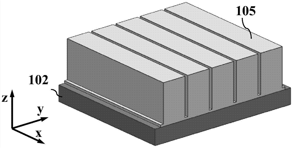
[0028] refer to figure 2 , this example includes from bottom to top: a lower electrode 102 , an absorption region 103 , an upper electrode 104 and a double-layer stress film 105 . The lower electrode 102 is made of a relaxed n-type Si material; the absorption region 103 is located on the lower electrode 102, and the absorption region 103 is made of a single-layer relaxed intrinsic SiGeSn composite material, and is arranged alternately with the gaps to form a fin structure; The upper electrode 104 is made of a relaxed p-type Si material, located on the upper surface of the absorption region 103, and its shape is the same as the fin shape of the absorption region 103; the double-layer stress film 105 completely wraps the sides of the upper electrode 104 and the absorption region 103, so that Stress is generated in the absorption reg...
Embodiment 3
[0031] Embodiment 3, single-layer structure absorption region, strained SiGeSn fin photodetector of single-layer structure stress layer
[0032] refer to figure 1 , this example includes from bottom to top: a lower electrode 102 , an absorption region 103 and an upper electrode 104 . The lower electrode 102 is made of relaxed n-type polysilicon material, the upper electrode 104 is made of relaxed p-type polysilicon material, and the absorption region 103 is made of a single-layer relaxed intrinsic SiGeSn composite material, which is arranged alternately with the gaps to form a fin structure; The shape of the upper electrode 104 is the same as the fin shape of the absorption region 103 . The surface of the upper electrode 104 and part of the sides of the absorption region 103 are wrapped with a single-layer stress film 105, such as image 3 shown. The stress film generates stress in the absorption region 103 to realize band gap adjustment of the absorption region 103 and inc...
PUM
 Abstract
Description
Claims
Application Information