Transverse IV-clan element quantum well photoelectric detector and preparation method

A photodetector and quantum well technology, applied in the field of photodetectors, can solve the problems of GeSn difficulty, material quality and thermal stability deterioration, difficulty in wide-ranging band gap adjustment, etc., to improve the band gap adjustment effect and price of materials. Inexpensive, Enhanced Effect of Bandgap Tuning Effect of Materials

Active Publication Date: 2015-10-28
XIDIAN UNIV
View PDF3 Cites 23 Cited by
  • Summary
  • Abstract
  • Description
  • Claims
  • Application Information

AI Technical Summary

Problems solved by technology

[0004] Theoretically, increasing the composition of Sn can reduce the band gap of GeSn material to zero, but because the solid solubility of Sn in Ge is very low, less than 1%, it is necessary to prepare high-quality, defect-free high-Sn components. GeSn is difficult
At present, the method of low-temperature epitaxial growth can only prepare GeSn materials with Sn composition of 20-25% [ECS Transactions, 41(7), pp.231, 2011; Photonics Research, 1(2).pp.69, 2013]
And as the Sn component increases, Sn atoms will segregate or segregate, and the material quality and thermal stability will deteriorate. Therefore, it is difficult to adjust the band gap in a wide range simply by increasing the Sn component.

Method used


Image

  • Transverse IV-clan element quantum well photoelectric detector and preparation method
  • Transverse IV-clan element quantum well photoelectric detector and preparation method
  • Transverse IV-clan element quantum well photoelectric detector and preparation method

Examples


Embodiment 1

[0028] Embodiment 1: Fabricate a lateral group IV element quantum well photodetector with the Sn composition of the quantum well being 0.3, the Ge composition of the potential barrier layer being 0, and the Si composition being 0.7.

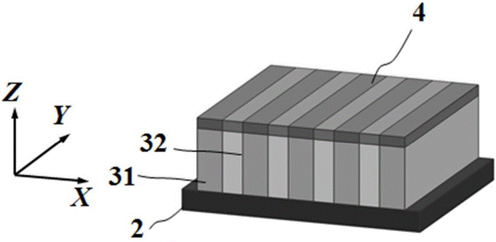
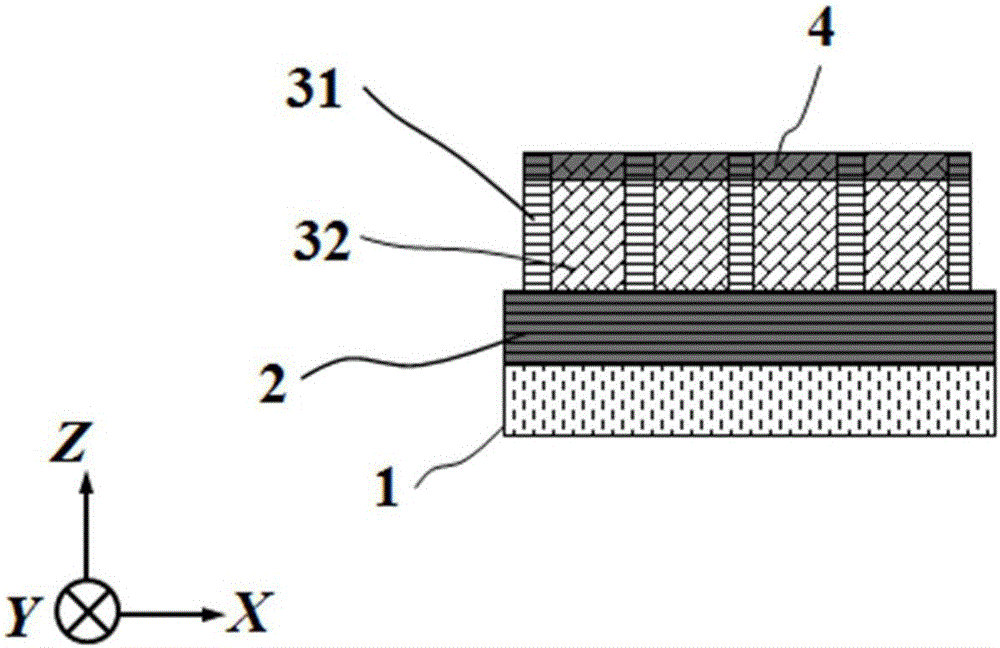
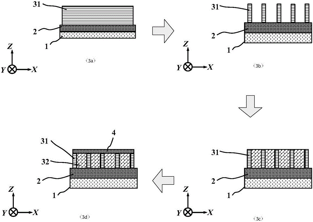
[0029] Step 1: On Si substrate 1, utilize molecular beam epitaxy process, use solid phosphorus, germanium and tin as evaporation source, use 10 -4 Pa pressure, in the environment of 180 ℃, grow n-type GeSn single crystal and relaxed intrinsic GeSn single crystal sequentially, in which the Sn composition is 0.3, and the Ge composition is 0.7. The grown n-type GeSn single crystal is Lower electrode 2, such as image 3 a.

[0030] Step 2: Etching the intrinsic GeSn single crystal into a lateral quantum well 31 under the masking effect of the photoresist by using the chloride-based ion group, such as image 3 b.

[0031] Step 3: using molecular beam epitaxy, using solid silicon, germanium and tin as evaporation sources, using 10 -4 Pa pressure, u...

Embodiment 2

[0034]Embodiment 2: Fabricate a lateral group IV element quantum well photodetector with the Sn composition of the quantum well being 0.15, the Ge composition of the potential barrier layer being 0.5, and the Si composition being 0.35.

[0035] Step 1: Sequential epitaxial relaxation of n-type GeSn single crystal and intrinsic GeSn single crystal

[0036] On the SOI substrate 1, with solid phosphorus, germanium and tin as evaporation sources, at a temperature of 190°C and a pressure of 10 -4 Pa environment, the epitaxial Sn composition is 0.15, the Ge composition is 0.85 n-type GeSn single crystal and the relaxation intrinsic GeSn single crystal, such as image 3 a.

[0037] Step 2: Etching quantum wells

[0038] Using chlorine-based ion groups as an etchant, under the masking effect of photoresist, longitudinally etch the relaxed intrinsic GeSn single crystal in step 1 epitaxy to form a quantum well 2 of GeSn single crystal material, such as image 3 b.

[0039] Step 3: E...

Embodiment 3

[0044] Embodiment 3: Fabricate a lateral group IV element quantum well photodetector in which the Sn composition of the quantum well is 0, the Ge composition of the potential barrier layer is 1, and the Si composition is 0.

[0045] Step A: using molecular beam epitaxy on a Ge substrate 1, using solid phosphorus, germanium and tin as evaporation sources, at a temperature of 200°C and a pressure of 10 -4 Pa environment, sequentially epitaxial n-type GeSn single crystal with Sn composition 0, Ge composition 1 and relaxed intrinsic GeSn single crystal, such as image 3 a.

[0046] Step B: Using chloride-based ion groups as etchant, under the masking effect of photoresist, etch intrinsic GeSn single crystal into lateral quantum wells, such as image 3 b.

[0047] Step C: Using molecular beam epitaxy, grow a SiGeSn single crystal material with a Si composition of 0, a Ge composition of 1, and a Sn composition of 0 in the gap between GeSn quantum wells, such as image 3 c. The p...


PUM


Abstract

The invention discloses a transverse IV-clan element quantum well photoelectric detector and mainly solves problems of high material toxicity and high cost of a conventional infrared photoelectric detector. The transverse IV-clan element quantum well photoelectric detector comprises a substrate (1), a bottom electrode (2), an absorption region (3), and a top electrode (4). A quantum well (31) uses a GeSn strain monocrystalline material with a Sn component more than or equal to 0 but less than 0.3. A barrier layer (32) uses a monocrystalline material with a Sn component more than or equal to 0 but less than 0.3 and a Ge component more than or equal to 0 but less than 1. The quantum well (31) and the barrier layer (32) are stacked transversely to form the absorption region arranged between the bottom electrode and the top electrode. According to the invention, SiGeSn monocrystalline material changes in size in an epitaxial process so as to generate transverse tensile strain in the GeSn quantum well material, thereby changing a GeSn material band gap and enlarging the spectral response range of the detector. The SiGeSn monocrystalline material can be used for producing large-scale integrated circuit.

Description

technical field [0001] The invention belongs to the technical field of microelectronic devices, and in particular relates to a photoelectric detector, which can be used in broadband communication, medical treatment, monitoring and automatic imaging. Background technique [0002] Photodetectors usually operate at low temperatures. Materials used in today's cooled infrared IR sensing systems include HgCdTe (MCT), InSb, PtSi, and doped Si. Quantum well infrared detectors are relatively new for IR sensor applications technology. HgCdTe is the most widely studied infrared detector for semiconductor alloy systems. So far, thermal imaging cameras based on HgCdTe focal plane detectors are still one of the mainstream development directions of infrared focal plane thermal imaging technology. Hg x Cd 1-x Te detector is currently the best mid-infrared detector, and the band gap can be continuously adjusted from 0-0.8eV by adjusting the Hg composition in the material. However, no mat...

Claims


Application Information

Patent Timeline
Patent Type & Authority Applications(China)
IPC IPC(8): H01L31/109H01L31/0352H01L31/028H01L31/18
CPCH01L31/028H01L31/035254H01L31/035263H01L31/03529H01L31/109H01L31/1804Y02P70/50
Inventor 韩根全张春福周久人汪银花张进城郝跃
Owner XIDIAN UNIV
Why Eureka
Try Eureka