Pixel structure, array substrate and liquid crystal display device

A pixel structure and thin-film transistor technology, applied in nonlinear optics, instruments, optics, etc., can solve problems such as inability to expand the viewing angle, screen flicker or afterimage, and affect product quality, so as to improve display quality, provide aperture ratio, and viewing angle Extended effect

Active Publication Date: 2015-03-18
BEIJING BOE OPTOELECTRONCIS TECH CO LTD
View PDF6 Cites 7 Cited by
  • Summary
  • Abstract
  • Description
  • Claims
  • Application Information

AI Technical Summary

Problems solved by technology

[0002] At present, the pixel structure of thin film transistor liquid crystal display (TFT-LCD) can improve the color shift through the self-compensation of liquid crystal, but the effect of expanding the viewing angle is limited, and it still cannot effectively expand the viewing angle in different dire

Method used


Image

  • Pixel structure, array substrate and liquid crystal display device
  • Pixel structure, array substrate and liquid crystal display device
  • Pixel structure, array substrate and liquid crystal display device

Examples


Embodiment Construction

[0021] The specific implementation manners of a pixel structure, an array substrate, and a liquid crystal display device provided by an embodiment of the present invention will be described in detail below with reference to the accompanying drawings.

[0022] The film thickness and shape of each layer in the drawings do not reflect the real scale of the array substrate, but are only intended to schematically illustrate the content of the present invention.

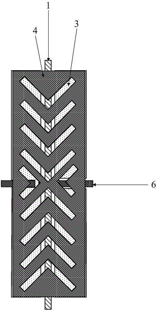
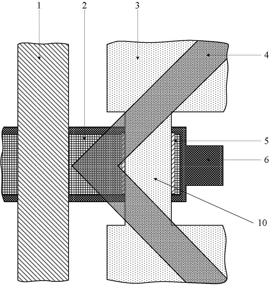
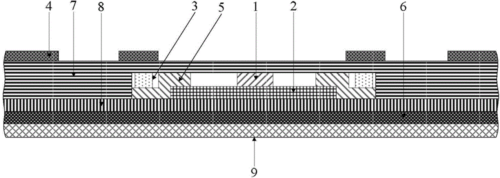
[0023] The embodiment of the present invention provides a pixel structure. In general, the pixel structure of the present invention mainly includes scanning lines 6, signal lines 1, slit electrodes 4, coupling electrodes 3 that can cooperate with the slit electrodes to form an electric field, and TFTs. A plurality of slits are formed on the slit electrode 4; wherein, the scanning lines 6 and the signal lines 1 overlap and define at least two sub-regions, and the coupling electrodes include at least two The sub-electrodes o...


PUM


Abstract

Provided are a pixel unit and an array substrate comprising the pixel unit, and a liquid crystal display device. The pixel unit comprises a scanning line (6), a signal line (1), a slit electrode (4), a coupling electrode (3) capable of cooperatively forming an electric field with the slit electrode (4), and a thin-film transistor, wherein a plurality of slits are formed on the slit electrode (4), the scanning line (6) and the signal line (1) are arranged crosswise and limit at least two sub-regions (I, II, III, IV). The coupling electrode (3) comprises at least two sub-electrodes respectively located in one of the sub-regions (I, II, III, IV). The slit electrode (4) corresponds to all the sub-regions (I, II, III, IV) and the extension directions of the slits located in different sub-regions (I, II, III, IV) are different. Therefore, enlarging the visual angles of different directions can effectively eliminate colour cast, and the aperture ratio can be effectively improved, thereby significantly improving the display quality.

Description

technical field [0001] The invention relates to liquid crystal display technology, in particular to a pixel structure, an array substrate, and a liquid crystal display device. Background technique [0002] At present, the pixel structure of thin-film transistor liquid crystal display (TFT-LCD) can improve color shift through self-compensation of liquid crystals, but the effect of expanding the viewing angle is limited, and it still cannot effectively expand the viewing angle in different directions. Moreover, in the traditional pixel structure, the gate / source parasitic capacitance is easy to change with the deviation of the process, which leads to different jump voltages in different display areas, and the screen may have adverse effects such as flickering or image sticking. product quality. Contents of the invention [0003] In view of this, the main purpose of the present invention is to provide a pixel structure, an array substrate, and a liquid crystal display device...

Claims


Application Information

Patent Timeline
IPC IPC(8): G02F1/1362G02F1/1368G02F1/1343G02F1/1345
CPCG02F1/1343G02F1/1368G02F1/133707G02F1/134363G02F1/134372
Inventor 蔡佩芝
Owner BEIJING BOE OPTOELECTRONCIS TECH CO LTD
Why Eureka
Try Eureka