Circuit board, method for manufacturing circuit board, electronic device, electronic apparatus, and moving object

A technology for circuit substrates and ceramic substrates, applied in the field of moving bodies, can solve the problems of insufficient adhesion between conductor parts and ceramic substrates, peeling of conductor parts, disconnection of conductor parts, etc.

Inactive Publication Date: 2015-03-18
SEIKO EPSON CORP
View PDF5 Cites 2 Cited by
  • Summary
  • Abstract
  • Description
  • Claims
  • Application Information

AI Technical Summary

Problems solved by technology

[0005] However, in conventional circuit boards, the adhesion between the conductor part and the ceramic substrate is not sufficiently obtained, and there are problems such as peeling of the conductor part or disconnection of the conductor part.
In addition, in the manufacture of circuit boards, there is also a problem that copper flows out and wiring shorts occur.

Method used


Image

  • Circuit board, method for manufacturing circuit board, electronic device, electronic apparatus, and moving object
  • Circuit board, method for manufacturing circuit board, electronic device, electronic apparatus, and moving object
  • Circuit board, method for manufacturing circuit board, electronic device, electronic apparatus, and moving object

Examples


Embodiment Construction

[0040] Hereinafter, the circuit board, the method for manufacturing the circuit board, and the electronic device of the present invention will be described in detail based on preferred embodiments shown in the drawings.

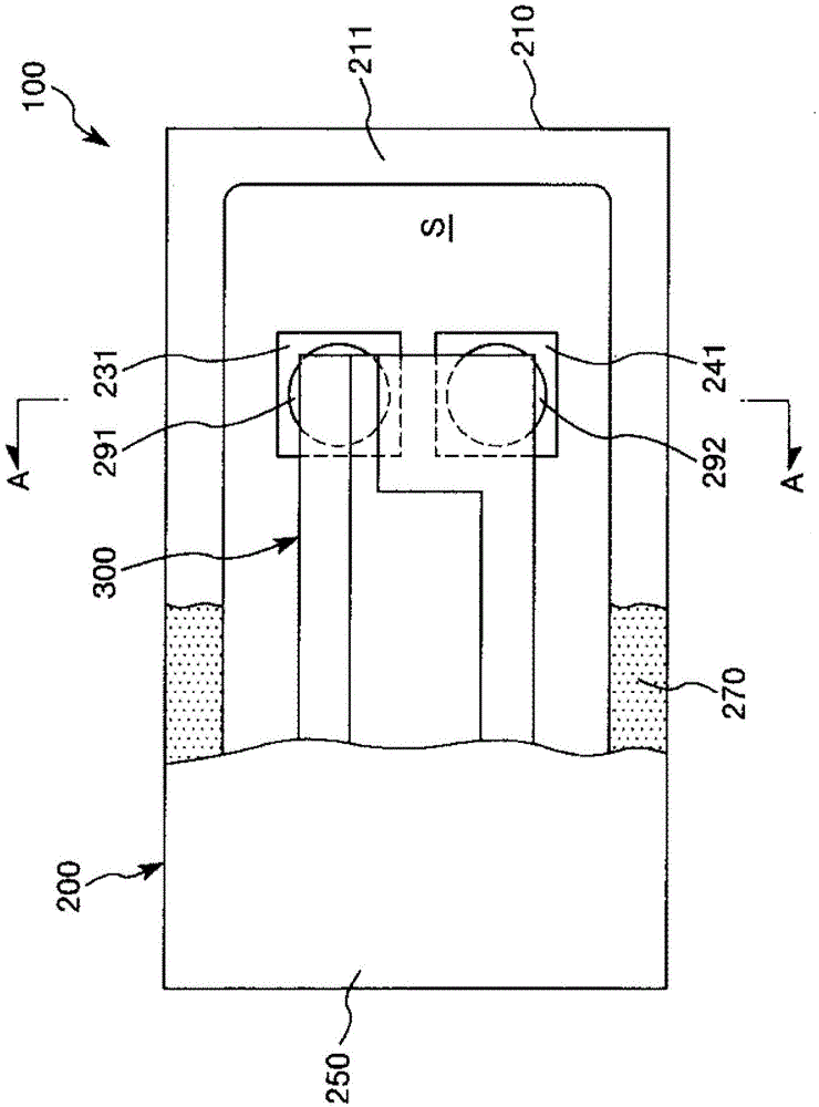
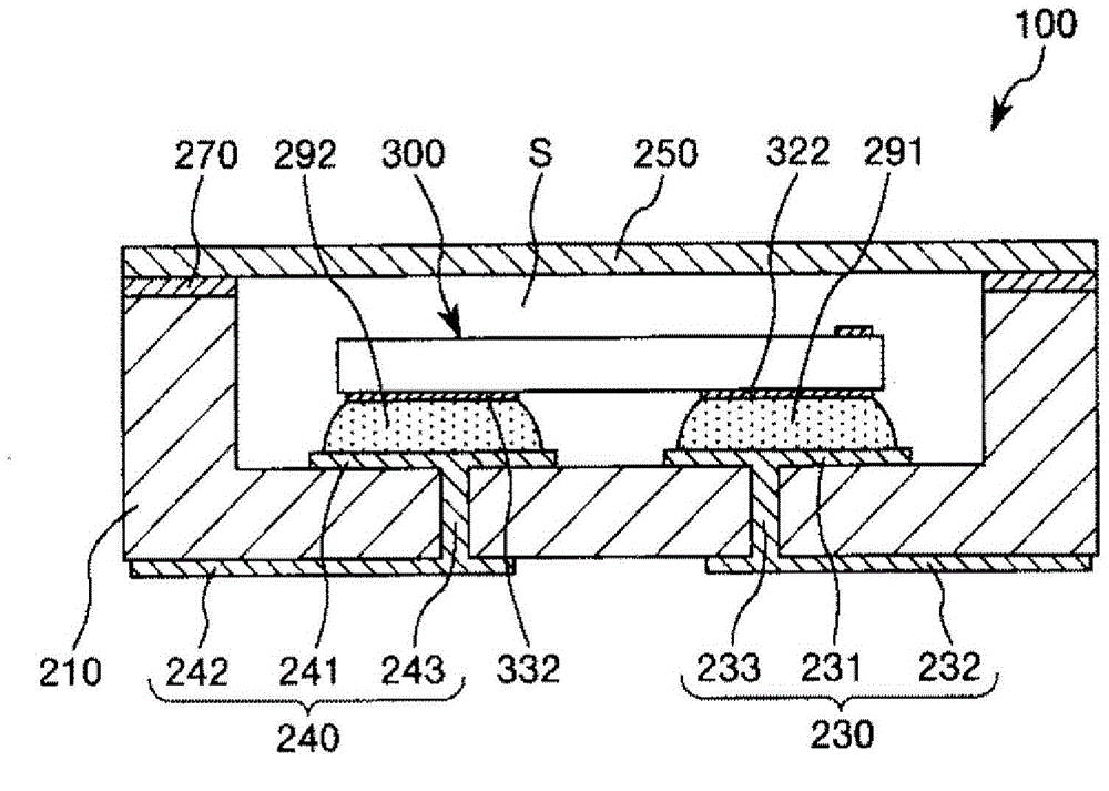
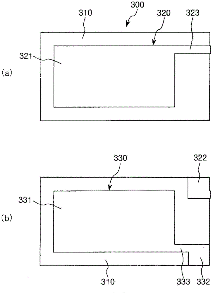
[0041] figure 1 is the top view of the electronic device, figure 2 yes figure 1 The A-A line sectional view in, image 3 yes figure 1 The shown electronic device has a top view of the vibrating element, Figure 4 yes figure 1 The illustrated electronic device has a partial cross-sectional view of a circuit substrate. In addition, in the following, for the convenience of explanation, the figure 1 The near front side of the paper in and figure 2 The upper side in is referred to as "upper", and the figure 1 the inside of the paper in and figure 2 The lower side in is called "lower".

[0042] 1. Electronic devices

[0043] First, the electronic device of the present invention (electronic device including the circuit board of the present invention) w...


PUM

PropertyMeasurementUnit
thicknessaaaaaaaaaa
sizeaaaaaaaaaa
sizeaaaaaaaaaa

Abstract

A circuit board includes a ceramics substrate composed of ceramics and a conductor portion provided on the ceramics substrate. The conductor portion is composed of a stacked body including, in order from the ceramics substrate side, an under layer that contains a Group 6 element and a glass material, and a metal layer that contains a low-melting-point metal. A portion of the low-melting-point metal constituting the metal layer migrates to the under layer.

Description

technical field [0001] The present invention relates to a circuit board, a method for manufacturing the circuit board, an electronic device, electronic equipment, and a mobile body. Background technique [0002] Conventionally, electronic devices are known in which electronic components such as vibration elements mounted on a circuit board are accommodated in a package. [0003] A circuit board on which electronic components are mounted has a structure in which wiring (conductor portions) are arranged on a ceramic substrate. [0004] Generally, such a circuit board is produced by arranging a conductive composition containing copper, tungsten, etc. on a green sheet and then firing it (for example, refer to Patent Document 1). [0005] However, in conventional circuit boards, the adhesiveness between the conductor part and the ceramic substrate is not sufficiently obtained, and there are problems such as peeling of the conductor part or disconnection of the conductor part. I...

Claims


Application Information

Patent Timeline
Patent Type & Authority Applications(China)
IPC IPC(8): H01L23/02H01L23/48H01L21/60
CPCH05K3/4644H05K1/181H05K1/0306H05K3/388H05K1/09H05K1/115H05K3/381H05K1/092H05K1/183H05K2203/1131H01L2224/16225
Inventor 宫尾哲郎大槻哲也石上秀树盐原幸彦中村英文
Owner SEIKO EPSON CORP
Why Eureka
Try Eureka