

HEMT device and manufacturing method of HEMT device
A device and gate technology, which is applied in the field of HEMT devices and their manufacturing, can solve the problems of reducing the high-frequency performance and breakdown performance of the device, reducing the reliability and yield of the device, and increasing the gate leakage current, so as to improve the high-frequency performance, reducing etch damage, shortening gate-source and gate-drain distances
- Summary
- Abstract
- Description
- Claims
- Application Information
AI Technical Summary
Problems solved by technology
Method used
Image

Examples
Embodiment 1
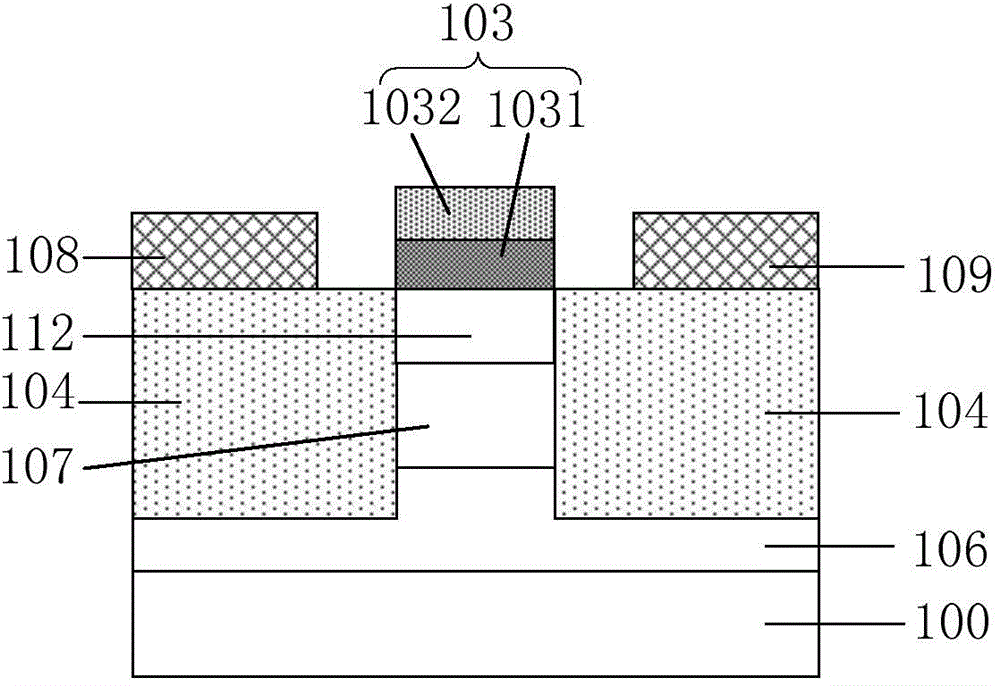
[0065] figure 1 A schematic structural diagram of the HEMT device provided by Embodiment 1 of the present invention is shown. Such as figure 1 As shown, the structure of the HEMT device shown includes: a substrate 100; an active region 106 formed on the substrate 100; a barrier region 107 formed on the active region 106; a barrier region 112 formed on the barrier region 107 Above, the gate 103 is formed on the barrier region 112; the low resistance region 104 is formed on both sides of the gate 103, wherein the low resistance region 104 is formed by a self-alignment process with the gate 103 as a mask, and the The low-resistance region 104 has doped particles, and the peak value of the concentration of the doped particles in the vertical direction is located at the part corresponding to the active region 106 or the part corresponding to the barrier region 107; and, the source electrode 108 and the drain 109 are respectively formed on the low resistance region 104 on both sid...
Embodiment 2
[0118] Image 6 It is a cross-sectional view of the structure of the HEMT device provided by Embodiment 2 of the present invention, such as Image 6 shown. Image 6 The same elements as in Fig. 3g are designated with the same reference numerals.
[0119] The structure of the HEMT device shown includes: a substrate 100; a buffer layer 110 formed on the substrate 100; an active region 106 formed on the buffer layer 110; a barrier region 107 formed on the active region 106; The barrier region 112 is formed on the barrier region 107, the gate 103 is formed on the barrier region 112; the gate spacers 113 and 114 are respectively located on both sides of the gate 103; the low resistance region 104 is formed on both sides of the gate 103 side, wherein the low-resistance region 104 is formed by a self-aligned process with the gate 103 as a mask, and the low-resistance region 104 has doped particles, and the peak value of the concentration of the doped particles in the vertical direc...
Embodiment 3
[0141] Figure 8 It is a cross-sectional view of the structure of the HEMT device provided by Embodiment 3 of the present invention, such as Figure 8 As shown, the HEMT device provided in the third embodiment includes: a substrate 201; a buffer layer 202, the buffer layer 202 is formed on the substrate 201; an active region 210, the active region 210 is formed on the buffer layer 202; barrier region 211, the barrier region 211 is formed on the active region 210; barrier region 212, the barrier region 212 is formed on the barrier region 211; gate 206, the gate 206 is formed on the barrier region 212; Pole sidewalls 215 and 216, the gate sidewalls 215 and 216 are formed on both sides of the gate 206 or formed on both sides of the gate 206 and on the gate 206; the low resistance region 207 is formed on both sides of the gate 203, wherein , the low-resistance region 207 is formed by a self-alignment process with the gate 206 as a mask, and the low-resistance region 207 has doped...
PUM
 Abstract
Description
Claims
Application Information