
T-shaped source-drain compound field plate power device
A power device and compound field technology, applied in the field of microelectronics, can solve the problems of reducing device yield, increasing device difficulty, cumbersome process debugging, etc., to improve reliability, improve forward and reverse breakdown voltage, and improve reverse The effect on the breakdown voltage
- Summary
- Abstract
- Description
- Claims
- Application Information
AI Technical Summary
Problems solved by technology
Method used
Image

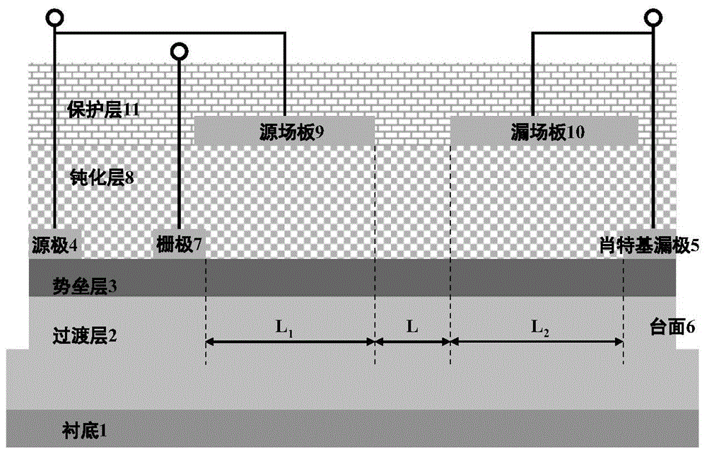
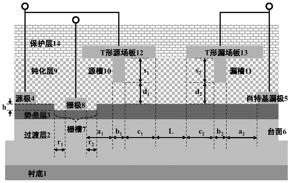
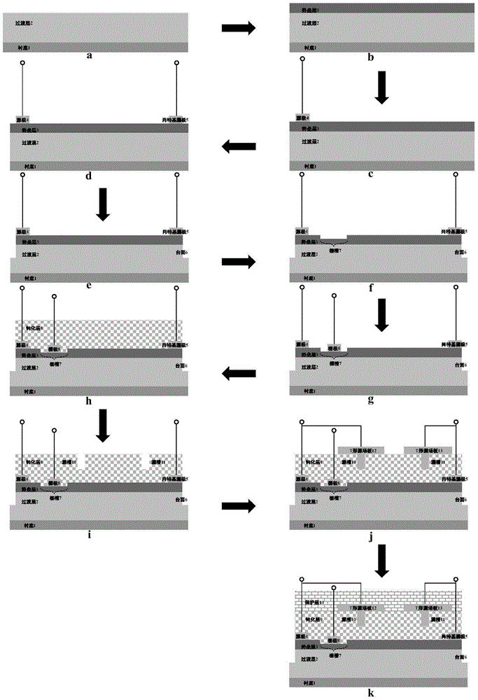
Examples
Embodiment 1
[0048] Embodiment one: making substrate is sapphire, and passivation layer is Al 2 o 3 , the protective layer is SiO 2 , the T-shaped source field plate and the T-shaped drain field plate are T-shaped source-drain compound field plate power devices composed of Ti / Mo / Au metal.
[0049] Step 1. On the sapphire substrate 1, make the transition layer 2 by epitaxial GaN material from bottom to top, such as image 3 a.
[0050] An undoped transition layer 2 with a thickness of 1 μm is epitaxially formed on the sapphire substrate 1 by metal organic chemical vapor deposition technology, and the transition layer is composed of GaN materials with thicknesses of 30 nm and 0.97 μm from bottom to top. The process conditions used for the epitaxial lower layer GaN material are: temperature 530°C, pressure 45 Torr, hydrogen gas flow rate 4400 sccm, ammonia gas flow rate 4400 sccm, gallium source flow rate 22 μmol / min; the process conditions for the epitaxial upper layer GaN material are: t...
Embodiment 2
[0071] Embodiment 2: The substrate is made of silicon carbide, and the passivation layer is SiO 2 , the protective layer is SiN, the T-shaped source field plate and the T-shaped drain field plate are a T-shaped source-drain composite field plate power device composed of Ti / Ni / Au metal.
[0072] Step 1. Epitaxially AlN and GaN materials on the silicon carbide substrate 1 to form the transition layer 2, such as image 3 a.
[0073] 1.1) Using metal-organic chemical vapor deposition technology to epitaxially undoped AlN material with a thickness of 50nm on the silicon carbide substrate 1; the process conditions for the epitaxy are: temperature is 1000°C, pressure is 45Torr, hydrogen flow rate is 4600sccm, The flow rate of ammonia gas is 4600 sccm, and the flow rate of aluminum source is 5 μmol / min;
[0074] 1.2) Using metal-organic chemical vapor deposition technology to epitaxially GaN material with a thickness of 2.45 μm on the AlN material to complete the fabrication of the ...
Embodiment 3
[0108] Embodiment three: the substrate is made of silicon, the passivation layer is SiN, and the protective layer is SiO 2 , the T-shaped source field plate and the T-shaped drain field plate are T-shaped source-drain composite field plate power devices composed of Ti / Pt / Au metal.
[0109] Step A. Epitaxial AlN and GaN materials on the silicon substrate 1 from bottom to top to make the transition layer 2, such as image 3 a.
[0110] A1) Using metal-organic chemical vapor deposition technology at a temperature of 800° C., a pressure of 40 Torr, a flow rate of hydrogen gas of 4000 sccm, a flow rate of ammonia gas of 4000 sccm, and a flow rate of aluminum source of 25 μmol / min, the epitaxy on the silicon substrate 1 AlN material with a thickness of 200nm;
[0111] A2) Using metal-organic chemical vapor deposition technology at a temperature of 980°C, a pressure of 45 Torr, a flow rate of hydrogen gas of 4000 sccm, a flow rate of ammonia gas of 4000 sccm, and a flow rate of gal...
PUM
 Abstract
Description
Claims
Application Information