Super-junction schottky diode

a super-junction, schottky diode technology, applied in the direction of semiconductor devices, basic electric elements, electrical apparatus, etc., can solve the problems of large forward voltage and reverse recovery time of schottky diodes, large reverse leakage current and poor temperature characteristics, and increase of forward conduction loss, etc., to achieve a smaller forward voltage, better reverse breakdown characteristic, and large forward current

Inactive Publication Date: 2018-01-25
UNIV OF ELECTRONICS SCI & TECH OF CHINA +1
View PDF2 Cites 6 Cited by
  • Summary
  • Abstract
  • Description
  • Claims
  • Application Information

AI Technical Summary

Benefits of technology

[0009]Some beneficial effects of the present invention are as follow. Compared to the existing super-junction schottky diode, the structure of this invention has a larger forward current, a smaller forward voltage, and a better reverse breakdown characteristic.

Problems solved by technology

However, PN junction diodes have a larger forward voltage and a longer reverse recovery time.
However, schottky diodes have a larger reverse leakage current and a poor temperature characteristic.
In order to improve the breakdown voltage of a schottky diode, the thickness of drift region must be enhanced and the doping concentration of drift region must be reduced, which leads to an increase of forward conduction loss.
However, the schottky junctions existing in schottky diodes are located on the surface of the devices, so that the current capacity of the schottky diode is limited since the surface area is limited.

Method used


Image

  • Super-junction schottky diode
  • Super-junction schottky diode
  • Super-junction schottky diode

Examples


embodiment 1

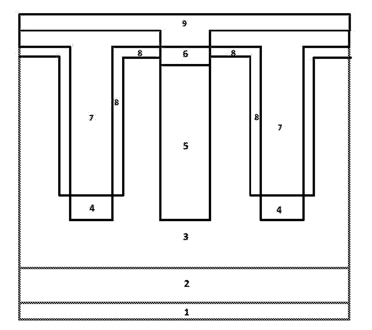
[0015]As shown in FIG. 1, the first embodiment of the present invention provides a super-junction schottky diode.

[0016]FIG.1 illustrates a super-junction schottky diode in accordance with thee present invention. The super-junction schottky diode includes: a metallized cathode electrode 1, a N+ substrate 2, an N-type drift region 3 and a metalized anode electrode 9. Said N-type drift region 3 includes a P-type buried layer 4, a P-type column 5, a P+ heavily doped region 6, an N-type lightly doped region 8 and a trench 7. The P-type buried layer 4 is under the trench 7, and the top surface of the P-type buried layer 4 contacts with the bottom surface of the trench 7. The P-type column 5 is located between two adjacent trenches 7. The P+ heavily doped region 6 is disposed above the P-type column 5 and the bottom surface of the heavily doped region 6 contacts the top surface of the P-type column 5. The N-type lightly doped region 8 is located on the side of the trench 7 and on the top s...

embodiment 2

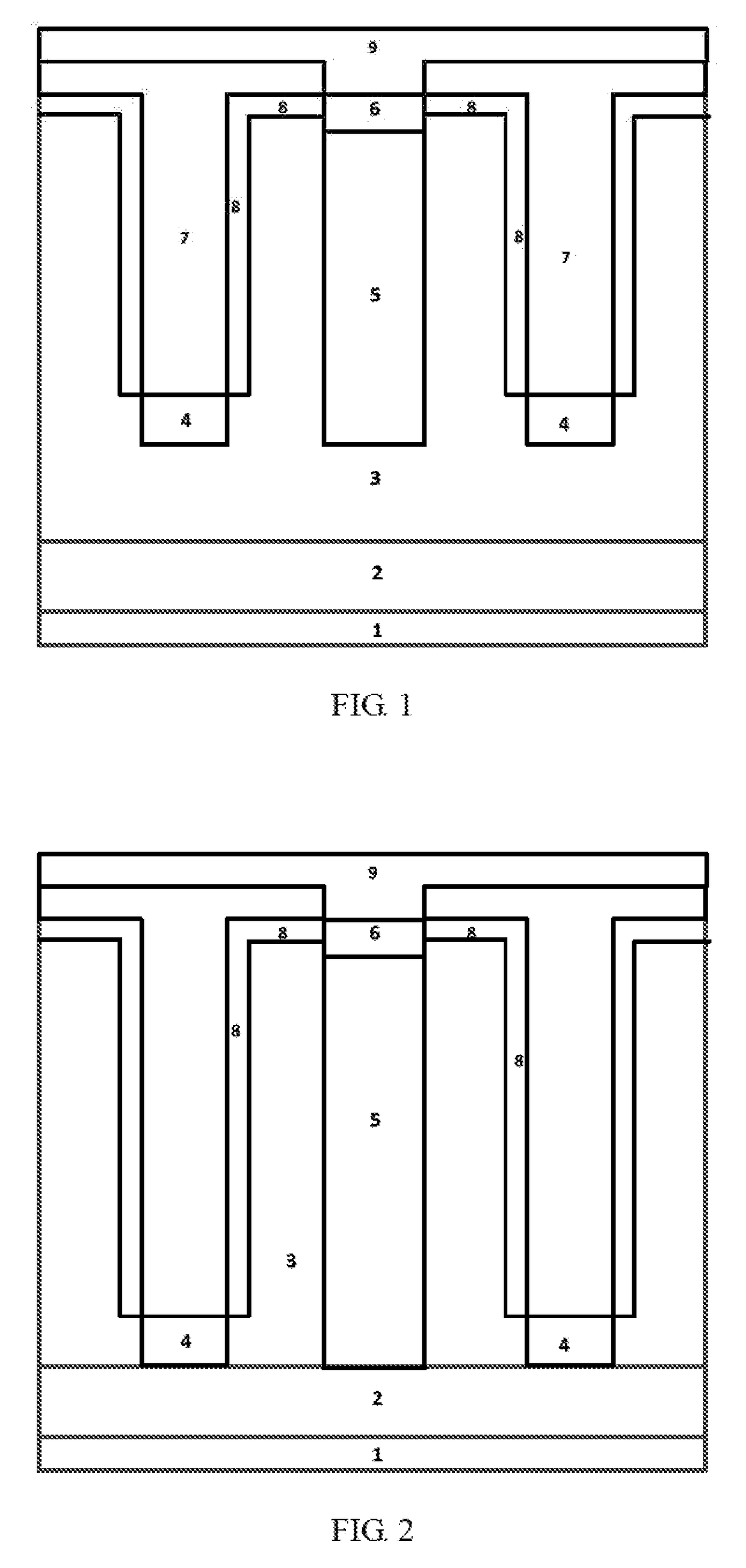
[0030]As shown in FIG. 2, based on the embodiment 1, the P-type column 5 and the trench 7 are extended. The bottom surfaces of both P-type column 5 and trench 7 touch the substrate 2. The beneficial effect of this embodiment is that the reverse breakdown voltage and leakage current of the device can be improved further.

embodiment 3

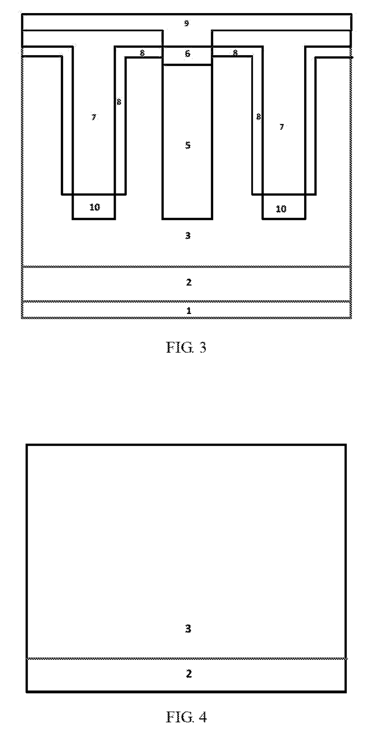
[0031]As shown in FIG. 3, based on the embodiment 1, the P-type buried layer 4 is replaced with the thick oxide layer 10. The breakdown can he prevented to occur at the bottom of the trench 7 and thus the reverse breakdown voltage of the device can be unproved.

[0032]In addition, other semiconductor materials such as silicon carbide, gallium arsenide, indium phosphide and germanium silicon can be used to replace silicon in manufacturing.


PUM


Abstract

The present invention relates to the field of semiconductor technology, particularly to a super-junction schottky diode. According to the present invention, the effective area of schottky junction is increased by forming the schottky junction in the trench located in the body of the device. Therefore, the current capacity of this novel schottky diode can be greatly improved. In addition, a super-junction structure is used to improve the device's reverse breakdown voltage and reduce the reverse leakage current. The super-junction schottky diode provided in the present invention can achieve a larger forward current, a lower on-resistance and a better reverse breakdown characteristic.

Description

CROSS REFERENCE[0001]The present application is based on, and claims priority from, Chinese application number 201610596069.4, filed on Jul. 25, 2016, the disclosure of which is hereby incorporated by reference herein in its entirety.TECHNICAL FIELD OF THE INVENTION[0002]The present invention relates to the technical field of semiconductor devices, particularly to a super-junction schottky diode.BACKGROUND OF THE INVENTION[0003]Diodes are one of the most commonly used electronic devices. The types of traditional diodes are schottky diodes and PN junction diodes. PN junction diodes can withstand high reverse blocking voltage and has better stability. However, PN junction diodes have a larger forward voltage and a longer reverse recovery time. Schottky diodes are based on the principle of metal-semiconductor junction. Schottky diodes have a lower forward voltage and a faster reverse recovery since it has no minority carrier accumulation during the forward conduction. However, schottky...

Claims


Application Information

Patent Timeline
Patent Type & Authority Applications(United States)
IPC IPC(8): H01L29/872H01L29/66H01L29/15
CPCH01L29/872H01L29/66143H01L29/158H01L29/157H01L29/0634H01L29/47H01L21/26586H01L29/0619H01L29/1608
Inventor REN, MINLIN, YUCIBAO, HUIPINGLUO, LEILI, ZEHONGZHANG, BO
Owner UNIV OF ELECTRONICS SCI & TECH OF CHINA
Why Eureka
Try Eureka