A planar metal oxide semiconductor diode with adjustable turn-on voltage

A technology of oxide semiconductor and turn-on voltage, which is applied in the direction of semiconductor devices, circuits, electrical components, etc., can solve problems such as limiting the application of devices, and achieve small conduction voltage drop, small reverse leakage current, and adjustable turn-on voltage Effect

Inactive Publication Date: 2019-03-29
UNIV OF ELECTRONICS SCI & TECH OF CHINA
View PDF5 Cites 0 Cited by
  • Summary
  • Abstract
  • Description
  • Claims
  • Application Information

AI Technical Summary

Problems solved by technology

However, once the existing diode is prepared, its forward voltage is fixed, which limits the application of the device to a certain extent.

Method used


Image

  • A planar metal oxide semiconductor diode with adjustable turn-on voltage
  • A planar metal oxide semiconductor diode with adjustable turn-on voltage
  • A planar metal oxide semiconductor diode with adjustable turn-on voltage

Examples


Embodiment Construction

[0013] The present invention is described in detail below in conjunction with accompanying drawing

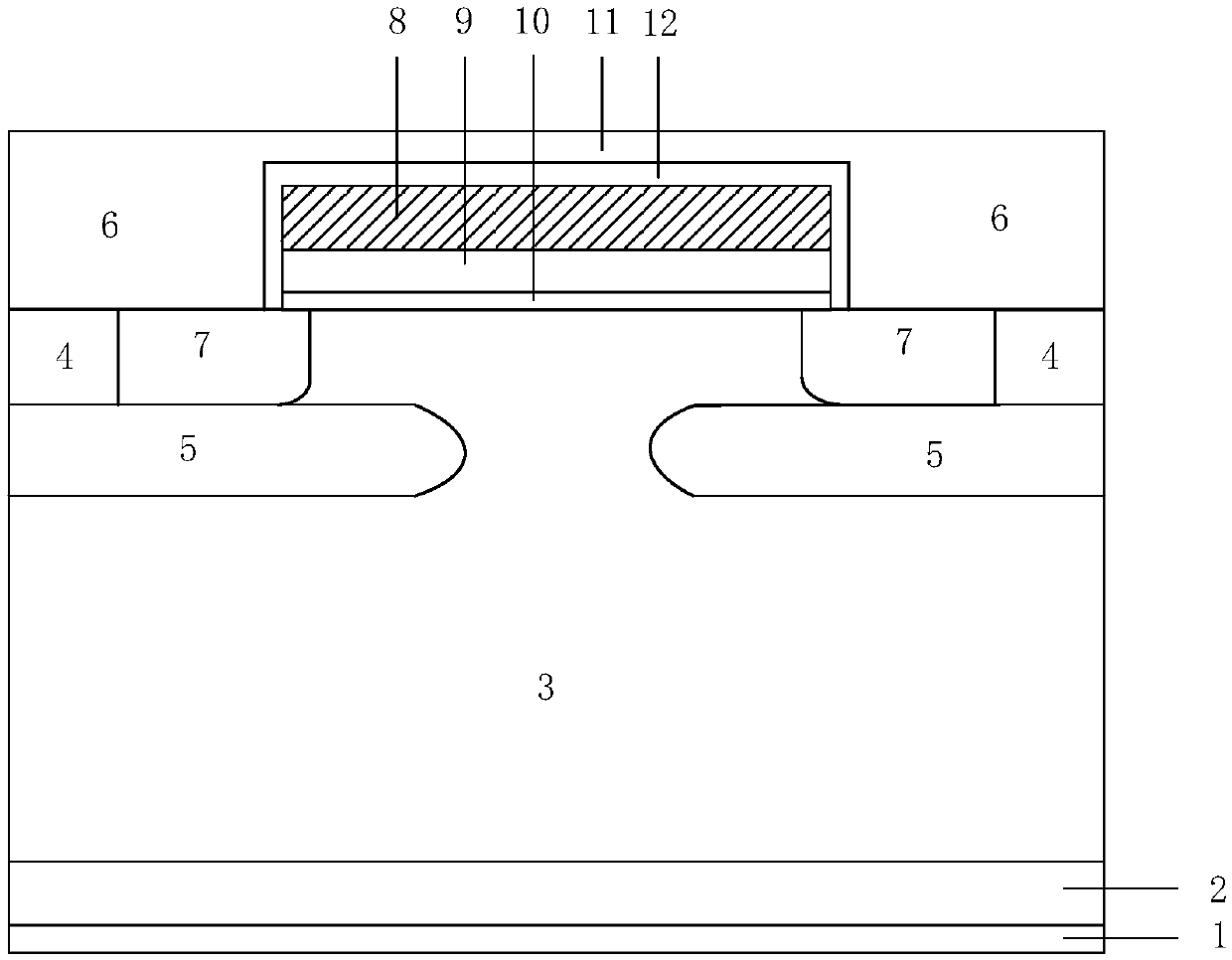
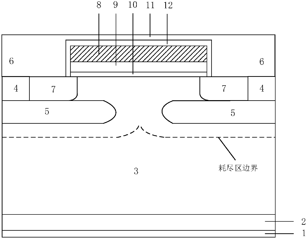
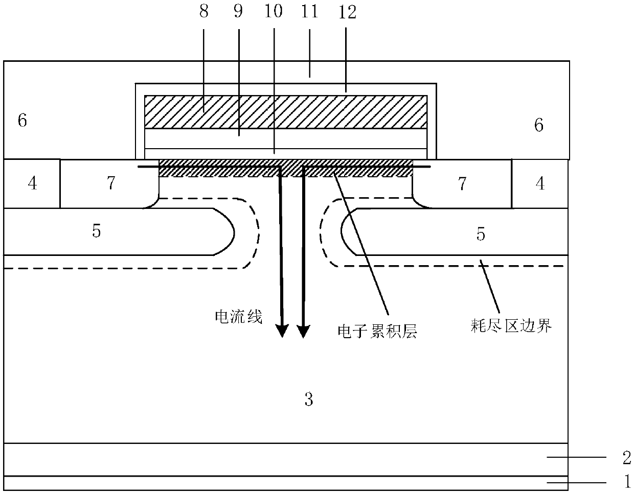
[0014] Such as figure 1 As shown, a planar metal oxide semiconductor diode with adjustable turn-on voltage of the present invention includes an N-type heavily doped single crystal silicon substrate 2, an N - the epitaxial layer 3 and the cathode electrode 1 located on the lower surface of the N-type heavily doped single crystal silicon substrate 2; the N-type epitaxial layer 3 has N-type heavily doped regions 7 on both sides of the upper layer, and the N-type heavily doped The lower surface of the region 7 is connected with a P-type buried layer 5; the side of the N-type heavily doped region 7 is a P-type heavily doped region 4; the middle part of the upper surface of the N- epitaxial layer 3 has a planar gate structure, and the planar The gate structure includes a silicon dioxide gate oxide layer 10, a nitride dielectric layer 9 and a polysilicon gate electrode 8; both sides ...


PUM


Abstract

The invention relates to the semiconductor technology, and especially to a plane type metal oxide semiconductor diode with an adjustable threshold voltage. The diode of the invention includes an N type heavy doping single crystal silicon substrate, an N-epitaxial layer, a cathode electrode, and an anode electrode. Both sides of an upper layer of the N-epitaxial layer are provided with N type heavy doping regions. P type buried layers are connected to lower surfaces of the N type heavy doping regions. Metal regions are connected to the upper surfaces of the N type heavy doping regions and P type heavy doping regions. The middle part of the upper surface of the N-epitaxial layer is provided with a plane gate structure. The both sides of a lower surface of a silicon dioxide gate oxide layer are in contact with the upper surfaces of the N type heavy doping regions. A nitride dielectric layer is arranged on the upper surface of the silicon dioxide gate layer. The anode electrode is connected to the P type heavy doping regions through the metal regions and forms the ohmic contact with the P type buried layers. The plane type metal oxide semiconductor diode with the adjustable threshold voltage has the beneficial effects that the plane type metal oxide semiconductor diode has a larger forward current, a less conduction voltage drop and a less reverse leakage current, and the threshold voltage of a device in the conditions that the reverse breakdown voltage and the reverse leakage current are not influenced can be adjustable.

Description

technical field [0001] The invention relates to semiconductor technology, in particular to a planar metal oxide semiconductor diode with adjustable turn-on voltage. Background technique [0002] Diodes are one of the most commonly used electronic components. Traditional rectifier diodes are mainly Schottky rectifiers and PN junction rectifiers. Among them, the PN junction diode can withstand a high reverse blocking voltage and has good stability, but its forward conduction voltage drop is relatively large, and its reverse recovery time is relatively long. Schottky diodes are manufactured using the principle of metal-semiconductor junctions formed by metal-semiconductor contacts, and the on-state voltage drop is low. Due to the conduction of unipolar carriers, Schottky diodes have no excess minority carrier accumulation during forward conduction, and the reverse recovery is relatively fast. However, the reverse breakdown voltage of the Schottky diode is low, the reverse lea...

Claims


Application Information

Patent Timeline
Patent Type & Authority Patents(China)
IPC IPC(8): H01L29/861
CPCH01L29/861
Inventor 任敏陈哲曹晓峰李爽李泽宏张金平高巍张波
Owner UNIV OF ELECTRONICS SCI & TECH OF CHINA
Why Eureka
Try Eureka