Sub-vertical-structure gallium nitride Schottky barrier diode and manufacturing method thereof

A technology with vertical structure and Schottky potential, applied in semiconductor/solid-state device manufacturing, electrical components, circuits, etc., can solve problems such as large reverse leakage current, low reverse withstand voltage, and insufficient stability, and achieve reverse Effects of small leakage current, high reverse recovery speed, and moderate electric field intensity

Pending Publication Date: 2022-04-12
江西誉鸿锦材料科技有限公司
View PDF0 Cites 0 Cited by
  • Summary
  • Abstract
  • Description
  • Claims
  • Application Information

AI Technical Summary

Problems solved by technology

[0003] Schottky barrier diodes manufactured by traditional technology have technical problems of large reverse leakage current, low reverse withstand voltage and insufficient stability, so the manufacture of diodes with small reverse leakage current, high reverse withstand voltage and good stability is an urgent requirement of the market

Method used


Image

  • Sub-vertical-structure gallium nitride Schottky barrier diode and manufacturing method thereof
  • Sub-vertical-structure gallium nitride Schottky barrier diode and manufacturing method thereof
  • Sub-vertical-structure gallium nitride Schottky barrier diode and manufacturing method thereof

Examples


Embodiment 1

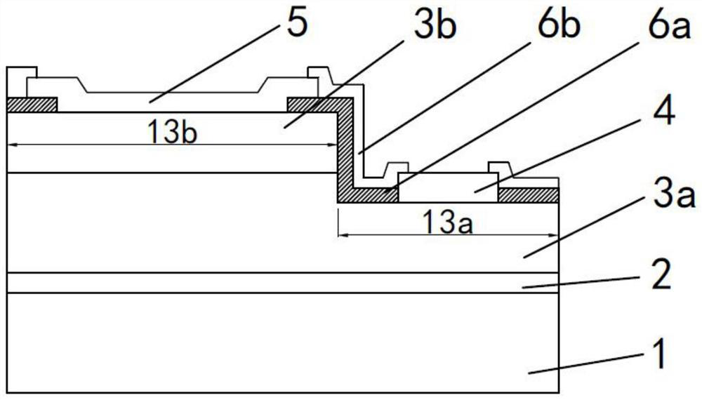
[0056] A gallium nitride Schottky barrier diode with sapphire as the substrate 1 disclosed in this embodiment uses C-plane sapphire with a thickness of 430 μm and an inclination of 0.15 degrees to the m-plane as the substrate. The specific manufacturing method is as follows:

[0057] Z1: The substrate 1 with a clean surface is placed on the tray of the MOCVD reaction furnace, and the surface is re-cleaned at a high temperature (1020°C) in a reducing atmosphere, and then the temperature is lowered to 550°C. gallium (TMGa) and ammonia (NH 3 ) as the raw material, the GaN material is grown at low temperature to form the GaN buffer layer 2, and then the temperature is gradually raised to crystallize the atomic sequence of the low-temperature GaN material. Wherein the thickness of the GaN buffer layer 2 is controlled at 10 nm.

[0058] Z2: epitaxial growth by metal organic chemical vapor phase epitaxy + - GaN epitaxial layers 3a and n - -GaN epitaxial layer 3b, pass into the rea...


PUM

PropertyMeasurementUnit
thicknessaaaaaaaaaa
thicknessaaaaaaaaaa
thicknessaaaaaaaaaa

Abstract

The sub-vertical structure gallium nitride Schottky barrier diode comprises a substrate (1), a buffer layer (2), an n < + >-GaN epitaxial layer (3a) and an n <->-GaN epitaxial layer (3b) which are sequentially arranged from bottom to top, the upper surface of the n <->-GaN epitaxial layer (3b) is a Schottky electrode arrangement region (13b), and the partially exposed part of the upper surface of the n < + >-GaN epitaxial layer (3a) is an ohmic electrode arrangement region (13a); the first insulation protection layer (6a) covers the ohmic electrode arrangement area (13a) and the Schottky electrode arrangement area (13b) and further covers the side wall face of a step formed by the n +-GaN epitaxial layer (3a) and the n-GaN epitaxial layer (3b), and the first insulation protection layer (6a) is provided with an ohmic electrode (4) in a window formed in the ohmic electrode arrangement area (13a). The first insulating protective layer (6a) is provided with a Schottky electrode (5) in a window formed in the Schottky electrode installation region (13b). According to the Schottky barrier diode, forward current is increased, and reverse breakdown voltage is improved.

Description

technical field [0001] The invention relates to the technical field of third-generation semiconductor materials and devices, in particular to a structure of a gallium nitride Schottky barrier diode with a sub-vertical structure and a manufacturing method thereof. Background technique [0002] Schottky barrier diode (SBD) is the key device of the rectifier circuit. It uses the unidirectional conductivity of the device to change the physical characteristics of the circuit such as voltage, current, frequency, and conduction state, and realizes functions such as power switch and power conversion. It is widely used in the industry. In the process of electronic upgrading, more and more attention and application have been paid to it. It is the core device in China's industrial processing, automobile manufacturing, wireless communication, consumer electronics, power transmission and transformation, and new energy applications. Therefore, higher requirements are put forward for its f...

Claims


Application Information

Patent Timeline
Patent Type & Authority Applications(China)
IPC IPC(8): H01L29/872H01L29/06H01L29/20H01L29/40H01L29/47H01L21/329
Inventor 邵春林闫怀宝闫发旺
Owner 江西誉鸿锦材料科技有限公司
Why Eureka
Try Eureka