SGT power MOS device integrated with barrier pinch-off diode and processing technology

A technology of MOS devices and diodes, applied in the field of semiconductor power devices, can solve the problems of power loss, large forward loss, and slow reverse recovery of SGT power MOS devices, so as to reduce the forward voltage drop and improve the reverse recovery speed. , The effect of reducing the forward conduction power consumption

Pending Publication Date: 2021-11-05
济南市半导体元件实验所
View PDF0 Cites 0 Cited by
  • Summary
  • Abstract
  • Description
  • Claims
  • Application Information

AI Technical Summary

Problems solved by technology

The presence of forward voltage drop results in power loss when the device conducts forward
[0004] Therefore, in order to solve the problems of slow reverse recovery and large forward loss of SGT power MOS devices, the present invention provides an SGT power MOS device with integrated barrier pinch-off diodes

Method used


Image

  • SGT power MOS device integrated with barrier pinch-off diode and processing technology
  • SGT power MOS device integrated with barrier pinch-off diode and processing technology
  • SGT power MOS device integrated with barrier pinch-off diode and processing technology

Examples


Embodiment Construction

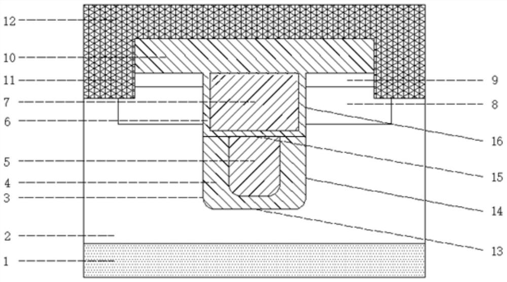
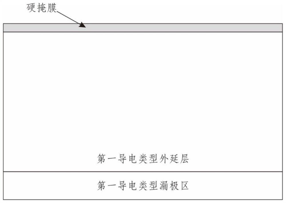
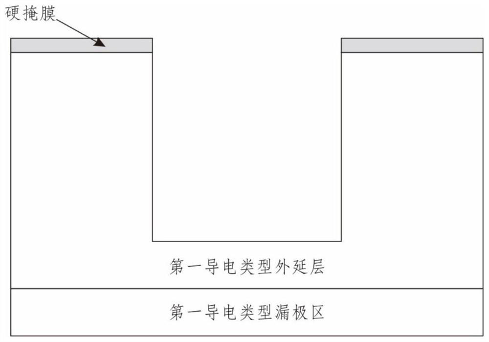
[0059] Below in conjunction with accompanying drawing and embodiment the present invention will be further described:

[0060] In order to clearly illustrate the technical features of this solution, the present invention will be described in detail below through specific implementation modes and in conjunction with the accompanying drawings. The following disclosure provides many different embodiments or examples for implementing different structures of the present invention. To simplify the disclosure of the present invention, components and arrangements of specific examples are described below. Furthermore, the present invention may repeat reference numerals and / or letters in different instances. This repetition is for the purpose of simplicity and clarity and does not in itself indicate a relationship between the various embodiments and / or arrangements discussed. It should be noted that components illustrated in the figures are not necessarily drawn to scale. Description...


PUM

PropertyMeasurementUnit
thicknessaaaaaaaaaa
depthaaaaaaaaaa
depthaaaaaaaaaa

Abstract

The invention discloses an SGT power MOS device integrated with a barrier pinch-off diode and a processing technology. The SGT power MOS device comprises a drain electrode region of a first conduction type and an epitaxial layer, a groove with an upward opening is arranged on the epitaxial layer, and a thick oxide layer filled with first polycrystalline silicon is arranged in the groove; a gate oxide layer filled with second polycrystalline silicon is arranged in the groove above the first polycrystalline silicon, and a well region layer of a second conductive type is arranged at the upper part of the epitaxial layer and around the groove; a source region layer is arranged on the well region layer, an insulating medium layer is arranged on the source region layer and the groove, a plurality of contact holes are formed in the insulating medium layer, and the contact holes are connected with the epitaxial layer, the well region layer and the source region layer; a metal region layer is laid above the insulating dielectric layer; and metal is arranged in the contact hole. According to the invention, the reverse recovery speed of the SGT power MOS device is improved, and the forward conduction power consumption of the SGT power MOS device is reduced.

Description

technical field [0001] The invention relates to an SGT power MOS device and a processing technology integrating potential barrier pinch-off diodes, and belongs to the technical field of semiconductor power devices. Background technique [0002] SGT power MOS devices can obtain lower on-resistance and lower conduction loss while improving device withstand voltage and saving device area; and the source polycrystalline of SGT power MOS devices can effectively reduce gate-drain capacitance, Increase the switching frequency of the device and reduce the switching loss of the device. As a result, SGT power MOS structure devices have a tendency to replace trench gate power MOS in the medium and low voltage field. However, when the SGT power MOS device is used as the low-side power switch of the DC voltage regulation module, the large forward injection effect of the parasitic body diode inside the device delays the reverse recovery time of the device, thus causing the operating freq...

Claims


Application Information

Patent Timeline
Patent Type & Authority Applications(China)
IPC IPC(8): H01L29/78H01L21/336
CPCH01L29/7813H01L29/7803H01L29/66734
Inventor 孙德福邢仟强李东华
Owner 济南市半导体元件实验所
Why Eureka
Try Eureka